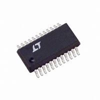
LTC1702IGN#TR Linear Technology, LTC1702IGN#TR Datasheet - Page 18

LTC1702IGN#TR
Manufacturer Part Number
LTC1702IGN#TR
Description
IC REG SW DUAL SYNC 2PH 24SSOP
Manufacturer
Linear Technology
Series
PolyPhase®r
Type
Step-Down (Buck)r
Datasheet
1.LTC1702CGN.pdf
(36 pages)
Specifications of LTC1702IGN#TR
Internal Switch(s)
No
Synchronous Rectifier
Yes
Number Of Outputs
2
Current - Output
1A, 25A
Frequency - Switching
550kHz
Voltage - Input
3 ~ 7 V
Operating Temperature
-40°C ~ 85°C
Mounting Type
Surface Mount
Package / Case
24-SSOP
Lead Free Status / RoHS Status
Contains lead / RoHS non-compliant
Voltage - Output
-
Power - Output
-
Available stocks
Company
Part Number
Manufacturer
Quantity
Price
APPLICATIONS
LTC1702
bypass capacitor gets exercised in three ways: its ESR
must be low enough to keep the initial drop as QT turns on
within reason (100mV or so); its RMS current capability
must be adequate to withstand the 4.6A
at the input and the capacitance must be large enough to
maintain the input voltage until the input supply can make
up the difference. Generally, a capacitor that meets the
first two parameters will have far more capacitance than is
required to keep capacitance-based droop under control.
In our example, we need 0.01Ω ESR to keep the input drop
under 100mV with a 10A current step and 4.6A
current capacity to avoid overheating the capacitor. These
requirements can be met with multiple low ESR tantalum
or electrolytic capacitors in parallel, or with a large mono-
lithic ceramic capacitor.
The two sides of the LTC1702 run off a single master clock
and are wired 180° out of phase with each other to
significantly reduce the total capacitance/ESR needed at
the input. Assuming 100mV of ripple and 10A output
current, we needed an ESR of 0.01Ω and 4.7A ripple
current capability for one side. Now, assume both sides
are running simultaneously with identical loading. If the
two sides switched in phase, all the loading conditions
would double and we’d need enough capacitance for
9.4A
phase, the input current is 4.8A
–3.2A
–6.4A
18
6.8A
3.6A
10A
10A
0
0
0
0
RMS
32%
32%
32% 18%
32%
and 0.005Ω ESR. With the two sides out of
18%
Figure 7. RMS Input Current
68%
68%
32%
32%
U
18%
18%
INFORMATION
U
RMS
W
—barely larger than
Q1 CURRENT, SIDE 1 ONLY
(FOR 1-PHASE, 2 SIDES:
MULTIPLY CURRENT BY 2)
CURRENT IN C
I
2 SIDES: I
BOTH SIDES EQUAL LOAD
2-PHASE OPERATION
CURRENT IN C
BOTH SIDES EQUAL LOAD
I
CIN
CIN
RMS
= 4.66A
= 4.8A
Q11 CURRENT
Q21 CURRENT
CIN
ripple current
RMS
RMS
= 9.3A
IN
IN
RMS
U
, (1-PHASE,
, SIDE 1 ONLY
,
RMS
ripple
)
1702 F07
Calculating RMS Current in C
A buck regulator like the LTC1702 draws pulses of
current from the input capacitor during normal opera-
tion. The input capacitor sees this as AC current, and
dissipates power proportional to the RMS value of the
input current waveform. To properly specify the capaci-
tor, we need to know the RMS value of the input current.
Calculating the approximate RMS value of a pulse train
with a fixed duty cycle is straightforward, but the LTC1702
complicates matters by running two sides simultaneously
and out of phase, creating a complex waveform at the
input.
To calculate the approximate RMS value of the input
current, we first need to calculate the average DC value
with both sides of the LTC1702 operating at maximum
load. Over a single period, the system will spend some
time with one top switch on and the other off, perhaps
some time with both switches on, and perhaps some
time with both switches off. During the time each top
switch is on, the current will equal that side’s full load
output current. When both switches are on, the total
current will be the sum of the two full load currents, and
when both are off, the current is effectively zero. Multiply
each current value by the percentage of the period that
the current condition lasts, and sum the results—this is
the average DC current value.
As an example, consider a circuit that takes a 5V input
and generates 3.3V at 3A at side 1 and 1.6V at 10A at
side 2. When a cycle starts, TG1 turns on and 3A flows
Figure SB1. Average Current Calculation
5.2
13
10
3
0
0
50%
A
TIME
16% 16% 18%
IN
B
C
D
1702 SB1
I
AVE
1702fa


