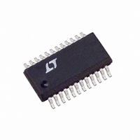
LTC1702IGN#TR Linear Technology, LTC1702IGN#TR Datasheet - Page 17

LTC1702IGN#TR
Manufacturer Part Number
LTC1702IGN#TR
Description
IC REG SW DUAL SYNC 2PH 24SSOP
Manufacturer
Linear Technology
Series
PolyPhase®r
Type
Step-Down (Buck)r
Datasheet
1.LTC1702CGN.pdf
(36 pages)
Specifications of LTC1702IGN#TR
Internal Switch(s)
No
Synchronous Rectifier
Yes
Number Of Outputs
2
Current - Output
1A, 25A
Frequency - Switching
550kHz
Voltage - Input
3 ~ 7 V
Operating Temperature
-40°C ~ 85°C
Mounting Type
Surface Mount
Package / Case
24-SSOP
Lead Free Status / RoHS Status
Contains lead / RoHS non-compliant
Voltage - Output
-
Power - Output
-
Available stocks
Company
Part Number
Manufacturer
Quantity
Price
APPLICATIONS
QB). This capacitance is composed of MOSFET channel
charge, actual parasitic drain-source capacitance and
Miller-multiplied gate-drain capacitance, but can be ap-
proximated as a single capacitance from gate to source.
Regardless of where the charge is going, the fact remains
that it all has to come out of V
on, and when the MOSFET is turned back off, that charge
all ends up at ground. In the meanwhile, it travels through
the LTC1702’s gate drivers, heating them up. More power
lost!
In this case, the power is lost in little bite-sized chunks, one
chunk per switch per cycle, with the size of the chunk set
by the gate charge of the MOSFET. Every time the MOSFET
switches, another chunk is lost. Clearly, the faster the
clock runs, the more important gate charge becomes as a
loss term. Old-fashioned switchers that ran at 20kHz could
pretty much ignore gate charge as a loss term; in the
550kHz LTC1702, gate charge loss can be a significant
efficiency penalty. Gate charge loss can be the dominant
loss term at medium load currents, especially with large
MOSFETs. Gate charge loss is also the primary cause of
power dissipation in the LTC1702 itself.
TG Charge Pump
There’s another nuance of MOSFET drive that the LTC1702
needs to get around. The LTC1702 is designed to use
N-channel MOSFETs for both QT and QB, primarily
because N-channel MOSFETs generally cost less and have
lower R
QB on is no big deal since the source of QB is attached to
PGND; the LTC1702 just switches the BG pin between
PGND and V
of QT is connected to SW which rises to V
on. To keep QT on, the LTC1702 must get TG one MOSFET
V
with the negative lead of the driver attached to SW (the
source of QT) and the V
separately at BOOST. An external 1µF capacitor C
nected between SW and BOOST (Figure 2) supplies power
to BOOST when SW is high, and recharges itself through
D
TG driver alive even as it swings well above V
of the bootstrap capacitor C
GS(ON)
CP
when SW is low. This simple charge pump keeps the
DS(ON)
above V
CC
than similar P-channel MOSFETs. Turning
. Driving QT is another matter. The source
CC
. It does this by utilizing a floating driver
U
CC
INFORMATION
U
lead of the driver coming out
CP
CC
needs to be at least 100
to turn the MOSFET gate
W
CC
CC
when QT is
. The value
U
CP
con-
times that of the total input capacitance of the topside
MOSFET(s). For very large external MOSFETs (or multiple
MOSFETs in parallel), C
the 1µF value.
INPUT SUPPLY
The BiCMOS process that allows the LTC1702 to include
large MOSFET drivers on-chip also limits the maximum
input voltage to 7V. This limits the practical maximum
input supply to a loosely regulated 5V or 6V rail. The
LTC1702 will operate properly with input supplies down to
about 3V, so a typical 3.3V supply can also be used if the
external MOSFETs are chosen appropriately (see the Power
MOSFETs section).
At the same time, the input supply needs to supply several
amps of current without excessive voltage drop. The input
supply must have regulation adequate to prevent sudden
load changes from causing the LTC1702 input voltage to
dip. In most typical applications where the LTC1702 is
generating a secondary low voltage logic supply, all of
these input conditions are met by the main system logic
supply when fortified with an input bypass capacitor.
Input Bypass
A typical LTC1702 circuit running from a 5V logic supply
might provide 1.6V at 10A at one of its outputs. 5V to 1.6V
implies a duty cycle of 32%, which means QT is on 32%
of each switching cycle. During QT’s on-time, the current
drawn from the input equals the load current and during
the rest of the cycle, the current drawn from the input is
near zero. This 0A to 10A, 32% duty cycle pulse train adds
up to 4.7A
last about 1.8µs—most system logic supplies have no
hope of regulating output current with that kind of speed.
A local input bypass capacitor is required to make up the
difference and prevent the input supply from dropping
drastically when QT kicks on. This capacitor is usually
chosen for RMS ripple current capability and ESR as well
as value.
The input bypass capacitor in an LTC1702 circuit is
common to both channels. Consider our 10A example
case with the other side of the LTC1702 disabled. The input
RMS
at the input. At 550kHz, switching cycles
CP
may need to be increased over
LTC1702
17
1702fa


