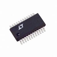
LTC1702IGN#TR Linear Technology, LTC1702IGN#TR Datasheet - Page 3

LTC1702IGN#TR
Manufacturer Part Number
LTC1702IGN#TR
Description
IC REG SW DUAL SYNC 2PH 24SSOP
Manufacturer
Linear Technology
Series
PolyPhase®r
Type
Step-Down (Buck)r
Datasheet
1.LTC1702CGN.pdf
(36 pages)
Specifications of LTC1702IGN#TR
Internal Switch(s)
No
Synchronous Rectifier
Yes
Number Of Outputs
2
Current - Output
1A, 25A
Frequency - Switching
550kHz
Voltage - Input
3 ~ 7 V
Operating Temperature
-40°C ~ 85°C
Mounting Type
Surface Mount
Package / Case
24-SSOP
Lead Free Status / RoHS Status
Contains lead / RoHS non-compliant
Voltage - Output
-
Power - Output
-
Available stocks
Company
Part Number
Manufacturer
Quantity
Price
ELECTRICAL CHARACTERISTICS
temperature range, otherwise specifications are T A = 25°C. V
SYMBOL
Switching Characteristics
f
Φ
DC
t
t
Feedback Amplifier
A
GBW
I
V
V
Current Limit Loop
A
I
Status Outputs
V
V
I
t
V
V
I
t
Note 1: Stresses beyond those listed under Absolute Maximum Ratings
may cause permanent damage to the device. Exposure to any Absolute
Maximum Rating condition for extended periods may affect device
reliability and lifetime.
Note 2: PV
the external MOSFETs used to ensure proper operation.
Note 3: All currents into device pins are positive; all currents out of device
pins are negative. All voltages are referenced to ground unless otherwise
specified.
OSC
DC
DC
NOV
ERR
IMAX
PGOOD
PGOOD
FAULT
FAULT
r
, t
VFB
MIN
MAX
VILIM
PGOOD
OLPG
FAULT
OLF
OSC2
MIN1
MIN2
MAX
f
CC
and BV
PARAMETER
Oscillator Frequency
Converter 2 Oscillator Phase
Minimum Duty Cycle
Minimum Duty Cycle
Maximum Duty Cycle
Driver Nonoverlap
Driver Rise/Fall Time
FB DC Gain
FB Gain Bandwidth
FB Sink/Source Current
MIN Comparator Threshold
MAX Comparator Threshold
I
I
PGOOD Trip Point
PGOOD Output Low Voltage
PGOOD Output Leakage
PGOOD Delay Time
FAULT Trip Point
FAULT Output Low Voltage
FAULT Output Current
FAULT Delay Time
LIM
MAX
Gain
CC
Source Current
(V
BOOST
– V
SW
) must be greater than V
GS(ON)
Test Circuit 1, C
CONDITIONS
Test Circuit 1, C
Relative to Converter 1 (Note 6)
V
V
Test Circuit 1, C
I
I
V
PGOOD = 1mA
V
V
I
V
V
MAX
MAX
FAULT
FB
FB
FB
FB
FB
FAULT
FB
The
< V
> V
Relative to Regulated V
< V
Relative to Regulated V
> V
= 0V, LTC1702C
= 0V, LTC1702I
of
CC
= 1mA
= 0V
MAX
MAX
PGOOD
FAULT
●
= 5V unless otherwise specified. (Note 3)
denotes specifications which apply over the full operating
to FAULT
to PGOOD
L
L
L
Note 4: Supply current in normal operation is dominated by the current
needed to charge and discharge the external MOSFET gates. This current
will vary with supply voltage and the external MOSFETs used.
Note 5: Supply current in shutdown is dominated by external MOSFET
leakage and may be significantly higher than the quiescent current drawn
by the LTC1702, especially at elevated temperature.
Note 6: This parameter is guaranteed by correlation and is not tested
directly.
Note 7: Rise and fall times are measured using 10% and 90% levels. Delay
and nonoverlap times are measured using 50% levels.
= 0pF
= 2000pF (Note 7)
= 2000pF (Note 7)
(Note 7)
OUT
OUT
(Note 7)
●
●
●
●
●
●
●
●
●
●
●
●
●
●
●
●
●
MIN
– 10
+ 10
475
815
±3
– 7
– 7
87
74
7
0
±0.1
0.03
0.03
TYP
550
180
±10
760
840
–10
–10
100
+ 15
– 10
– 5
10
90
40
12
85
25
40
25
LTC1702
MAX
–13
–14
+ 20
750
100
785
0.1
0.1
– 2
±1
93
80
UNITS
1702fa
3
DEG
MHz
kHz
mA
mV
mV
dB
dB
µA
µA
µA
µA
ns
ns
µs
µs
%
%
%
%
%
V
V


