THNCF512MDG Toshiba, THNCF512MDG Datasheet - Page 14
THNCF512MDG
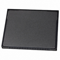
Manufacturer Part Number
THNCF512MDG
Description
MEMORY CARD COMPACT FLASH 512MB
Manufacturer
Toshiba
Datasheet
1.THNCF128MDG.pdf
(44 pages)
Specifications of THNCF512MDG
Memory Size
512MB
Memory Type
CompactFLASH
Lead Free Status / RoHS Status
Lead free / RoHS Compliant


2. Configuration and Status register (Address 202h)
Note:
CHGED
(CARD->)
SIGCHG
(HOST->)
IOIS8
(HOST->)
PWD
(HOST->)
INTR
(CARD->)
This register is used for observing the state of the card.
CHGED
Name
bit7
initial value → 00H
SIGCHG
R/W
R/W
R/W
R/W
bit6
R
R
This bit indicates that CREADY bit on Pin Replacement register is set to “1”. When CHGED bit is
set to “1”, −STSCHG pin is held “L” at the condition of SIGCHG bit set to “1” and the card
configured for the I/O interface.
This bit is set or reset by the host for enabling and disabling the status-change signal (
pin). When the card is configured I/O card interface and this bit is set “1”,
controlled by CHGED bit. If this bit is set to “0”,
The host sets this field to “1” when it can provide I/O cycles only with on 8 bit data bus (D7
When this bit is set to “1”, the card enters sleep state (Power Down mode). When this bit is reset
to “0”, the card transfers to idle state (active mode). RREADY bit on Pin Replacement Register
becomes BUSY when this bit is changed. RREADY will not become Ready until the power state
requested has been entered.
This bit indicates the internal state of the interrupt request. This bit state is available whether I/O
card interface has been configured or not. This signal remains true until the condition, which
caused the interrupt request, has been serviced. If the
disables interrupts, this bit is a zero.
IOIS8
bit5
TENTATIVE
bit4
0
bit3
0
Function
−
STSCHG pin is kept “H”.
PWD
bit2
−
IEN bit in the Device Control Register
THNCFxxxxDG Series
INTR
2004-05-18 14/44
bit1
−
STSCHG pin is
−
STSCHG
bit0
0
to
D0).
Related parts for THNCF512MDG
Image
Part Number
Description
Manufacturer
Datasheet
Request
R

Part Number:
Description:
Toshiba Semiconductor [TOSHIBA IGBT Module Silicon N Channel IGBT]
Manufacturer:
TOSHIBA Semiconductor CORPORATION
Datasheet:
Part Number:
Description:
TOSHIBA GTR MODULE SILICON NPN TRIPLE DIFFUSED TYPE
Manufacturer:
TOSHIBA Semiconductor CORPORATION
Datasheet:
Part Number:
Description:
TOSHIBA GTR Module Silicon N Channel IGBT
Manufacturer:
TOSHIBA Semiconductor CORPORATION
Datasheet:
Part Number:
Description:
TOSHIBA Intelligent Power Module Silicon N Channel IGBT
Manufacturer:
TOSHIBA Semiconductor CORPORATION
Datasheet:
Part Number:
Description:
TOSHIBA INTELLIGENT POWER MODULE SILICON N CHANNEL LGBT
Manufacturer:
TOSHIBA Semiconductor CORPORATION
Datasheet:
Part Number:
Description:
TOSHIBA IGBT Module Silicon N Channel IGBT
Manufacturer:
TOSHIBA Semiconductor CORPORATION
Datasheet:
Part Number:
Description:
TOSHIBA GTR MODULE SILICON N−CHANNEL IGBT
Manufacturer:
TOSHIBA Semiconductor CORPORATION
Datasheet:
Part Number:
Description:
TOSHIBA Intelligent Power Module Silicon N Channel IGBT
Manufacturer:
TOSHIBA Semiconductor CORPORATION
Datasheet:
Part Number:
Description:
TOSHIBA GTR Module Silicon N Channel IGBT
Manufacturer:
TOSHIBA Semiconductor CORPORATION
Datasheet:
Part Number:
Description:
TOSHIBA INTELLIGENT POWER MODULE
Manufacturer:
TOSHIBA Semiconductor CORPORATION
Datasheet:
Part Number:
Description:
TOSHIBA Intelligent Power Module Silicon N Channel IGBT
Manufacturer:
TOSHIBA Semiconductor CORPORATION
Datasheet:
Part Number:
Description:
TOSHIBA Intelligent Power Module Silicon N Channel IGBT
Manufacturer:
TOSHIBA Semiconductor CORPORATION
Datasheet:
Part Number:
Description:
TOSHIBA IGBT Module Silicon N Channel IGBT
Manufacturer:
TOSHIBA Semiconductor CORPORATION
Datasheet:
Part Number:
Description:
TOSHIBA Intelligent Power Module Silicon N Channel IGBT
Manufacturer:
TOSHIBA Semiconductor CORPORATION
Datasheet:
Part Number:
Description:
Toshiba Semiconductor [SILICON N CHANNEL 1GBT]
Manufacturer:
TOSHIBA Semiconductor CORPORATION
Datasheet: