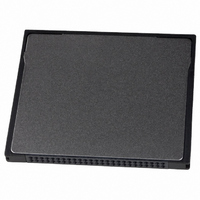
THNCF512MDG Toshiba, THNCF512MDG Datasheet - Page 6

THNCF512MDG
Manufacturer Part Number
THNCF512MDG
Description
MEMORY CARD COMPACT FLASH 512MB
Manufacturer
Toshiba
Datasheet
1.THNCF128MDG.pdf
(44 pages)
Specifications of THNCF512MDG
Memory Size
512MB
Memory Type
CompactFLASH
Lead Free Status / RoHS Status
Lead free / RoHS Compliant
Signal Description
A10 to A0
(PC Card Memory Mode)
A10 to A0
(PC Card I/O Mode)
A2 to A0
(True IDE Mode)
BVD1
(PC Card Memory Mode)
−
(PC Card I/O Mode)
−
(True IDE Mode)
BVD2
(PC Card Memory Mode)
−
(PC Card I/O Mode)
−
(True IDE Mode)
−CD1, −CD2
(PC Card Memory Mode)
−
(PC Card I/O Mode)
−
(True IDE Mode)
−
(PC Card Memory Mode)
−
(PC Card I/O Mode)
−
(True IDE Mode)
−
(PC Card Memory Mode)
−
(PC Card I/O Mode)
−
(True IDE Mode)
D15 to D00
(PC Card Memory Mode)
D15 to D00
(PC Card I/O Mode)
D15 to D00
(True IDE Mode)
STSCHG
PDIAG
SPKR
DASP
CD1,
CD1,
CE1,
CE1,
CS0,
CSEL
CSEL
CSEL
−
−
−
−
−
CE2
CE2
CS1
CD2
CD2
Signal Name
Dir
I/O
I/O
I/O
O
I
I
I
8,10,11,12,1
4,15,16,17,1
31,30,29,28,
27,49,48,47,
6,5,4,3,2,
18,19,20
23,22,21
Pin No.
8,19,20
26,25
7,32
TENTATIVE
46
45
39
Address signals. A10 is the most significant bit, A0 is the least
significant bit.
In True IDE Mode only A2~0 are available, the remaining address
lines should be grounded by the host.
This signal always outputs high, since battery voltage detection is
not supported.
This signal is asserted low to alert the host to changes in the
READY and Write Protect states; while the I/O interface is
configured .Its use is controlled by the Card Configuration and
Status Register.
In the True IDE Mode, this signal is bi-directional and used to show
diagnostic result in the Master/Slave handshake protocol.
This signal always outputs high, since battery voltage detection is
not supported.
This is the Binary Audio output signal. Since this card does not
support the Binary Audio function, this signal always outputs high.
This bi-directional signal is the Disk Active / Slave Present signal.
These Card Detect pins are connected to ground on the
CompactFlash Storage Card. They are used by the host to
determine that the CompactFlash Storage Card is fully inserted into
its socket.
These input signals are used both to select the card and to indicate
to the card whether a byte or a word operation is being performed.
Please refer to Access specifications.
In the True IDE Mode CS0 is the chip select for the task file
registers while CS1 is used to select the Alternate Status Register
and the Device Control Register.
This signal is not used for this mode.
This internally pulled up signal is used to configure this device as a
Master or a Slave when configured in the True IDE Mode.
When this pin is grounded, this device is configured as a Master.
When the pin is open, this device is configured as a Slave.
These lines carry the Data, Commands and Status information
between the host and the controller. D00 is the LSB of the Even
Byte of the Word.D08 is the LSB of the Odd Byte of the Word.
True IDE Mode, all Task File operations occur in byte mode on the
low order bus D00 to D07 while all data transfers are 16 bit using
D00 to D15.
Description
THNCFxxxxDG Series
2004-05-18 6/44


