ADC1415S125/DB,598 NXP Semiconductors, ADC1415S125/DB,598 Datasheet - Page 12
ADC1415S125/DB,598
Manufacturer Part Number
ADC1415S125/DB,598
Description
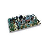
BOARD DEMO FOR ADC1415S125
Manufacturer
NXP Semiconductors
Type
A/Dr
Datasheets
1.ADC1415S125HNC15.pdf
(42 pages)
2.HSDC-ACC01DB.pdf
(32 pages)
3.ADC1415S125DB598.pdf
(2 pages)
Specifications of ADC1415S125/DB,598
Number Of Adc's
1
Number Of Bits
14
Sampling Rate (per Second)
125M
Data Interface
Serial, SPI™
Inputs Per Adc
1 Differential
Input Range
1 ~ 2 Vpp
Power (typ) @ Conditions
840mW @ 125Msps
Voltage Supply Source
Single Supply
Operating Temperature
-40°C ~ 85°C
Utilized Ic / Part
ADC1415S125
Product
Data Conversion Development Tools
Conversion Rate
125 MSPS
Resolution
14 bit
Interface Type
SMA
For Use With/related Products
ADC1415S125
Lead Free Status / RoHS Status
Lead free / RoHS Compliant
Lead Free Status / RoHS Status
Lead free / RoHS Compliant, Lead free / RoHS Compliant
Other names
568-5094


Table 8.
Symbol
Clock timing input: pins CLKP and CLKM
f
t
δ
t
t
CMOS Mode timing output: pins D13 to D0 and DAV
t
t
t
t
t
clk
lat(data)
d(s)
wake
PD
su
h
r
f
clk
Clock and digital output timing characteristics
Parameter
clock frequency
data latency
time
clock duty cycle DCS_EN = 1
sampling delay
time
wake-up time
propagation
delay
set-up time
hold time
rise time
fall time
10.2 Clock and digital output timing
Conditions
DCS_EN = 0
DATA
DAV
DATA
DAV
DATA
[2]
[2]
40
-
30
45
-
-
13.6
-
-
-
0.39
0.26
0.19
Min
ADC1410S065
[1]
-
13.5
50
50
0.8
76
14.9
4.2
12.5
3.4
-
-
-
Typ
65
-
70
55
-
-
16.4
-
-
-
2.4
2.4
2.4
Max
60
-
30
45
-
-
11.9
-
-
-
0.39
0.26
0.19
Min
ADC1410S080
-
13.5
50
50
0.8
76
12.9
3.6
9.8
3.3
-
-
-
Typ
80
-
-
70
55
-
-
14.4
-
-
2.4
2.4
2.4
Max
75
-
30
45
-
-
8.0
-
-
-
0.39
0.26
0.19
Min
ADC1410S105
-
13.5
50
50
0.8
76
10.8
3.3
6.8
3.1
-
-
-
Typ
105
-
70
55
-
-
12.4
-
-
-
2.4
2.4
2.4
Max
100
-
30
45
-
-
8.2
-
-
-
0.39
0.26
0.19
Min
ADC1410S125
-
13.5
50
50
0.8
76
9.7
3.4
5.6
2.8
-
-
-
Typ
125
-
70
55
-
-
11.3
-
-
-
2.4
2.4
2.4
Max
Unit
MHz
clock
cycles
%
%
ns
μs
ns
ns
ns
ns
ns
ns
ns
Related parts for ADC1415S125/DB,598
Image
Part Number
Description
Manufacturer
Datasheet
Request
R

Part Number:
Description:
Single 14-bit ADC
Manufacturer:
NXP Semiconductors
Datasheet:
Part Number:
Description:
NXP Semiconductors designed the LPC2420/2460 microcontroller around a 16-bit/32-bitARM7TDMI-S CPU core with real-time debug interfaces that include both JTAG andembedded trace
Manufacturer:
NXP Semiconductors
Datasheet:

Part Number:
Description:
NXP Semiconductors designed the LPC2458 microcontroller around a 16-bit/32-bitARM7TDMI-S CPU core with real-time debug interfaces that include both JTAG andembedded trace
Manufacturer:
NXP Semiconductors
Datasheet:
Part Number:
Description:
NXP Semiconductors designed the LPC2468 microcontroller around a 16-bit/32-bitARM7TDMI-S CPU core with real-time debug interfaces that include both JTAG andembedded trace
Manufacturer:
NXP Semiconductors
Datasheet:
Part Number:
Description:
NXP Semiconductors designed the LPC2470 microcontroller, powered by theARM7TDMI-S core, to be a highly integrated microcontroller for a wide range ofapplications that require advanced communications and high quality graphic displays
Manufacturer:
NXP Semiconductors
Datasheet:
Part Number:
Description:
NXP Semiconductors designed the LPC2478 microcontroller, powered by theARM7TDMI-S core, to be a highly integrated microcontroller for a wide range ofapplications that require advanced communications and high quality graphic displays
Manufacturer:
NXP Semiconductors
Datasheet:
Part Number:
Description:
The Philips Semiconductors XA (eXtended Architecture) family of 16-bit single-chip microcontrollers is powerful enough to easily handle the requirements of high performance embedded applications, yet inexpensive enough to compete in the market for hi
Manufacturer:
NXP Semiconductors
Datasheet:
Part Number:
Description:
The XA-S3 device is a member of Philips Semiconductors? XA(eXtended Architecture) family of high performance 16-bitsingle-chip microcontrollers
Manufacturer:
NXP Semiconductors
Datasheet:

Part Number:
Description:
The NXP BlueStreak LH75401/LH75411 family consists of two low-cost 16/32-bit System-on-Chip (SoC) devices
Manufacturer:
NXP Semiconductors
Datasheet:
Part Number:
Description:
The NXP LPC3130/3131 combine an 180 MHz ARM926EJ-S CPU core, high-speed USB2
Manufacturer:
NXP Semiconductors
Datasheet:
Part Number:
Description:
The NXP LPC3141 combine a 270 MHz ARM926EJ-S CPU core, High-speed USB 2
Manufacturer:
NXP Semiconductors
Part Number:
Description:
The NXP LPC3143 combine a 270 MHz ARM926EJ-S CPU core, High-speed USB 2
Manufacturer:
NXP Semiconductors

Part Number:
Description:
The NXP LPC3152 combines an 180 MHz ARM926EJ-S CPU core, High-speed USB 2
Manufacturer:
NXP Semiconductors
Part Number:
Description:
The NXP LPC3154 combines an 180 MHz ARM926EJ-S CPU core, High-speed USB 2
Manufacturer:
NXP Semiconductors