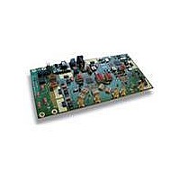
ADC1415S125/DB,598 NXP Semiconductors, ADC1415S125/DB,598 Datasheet - Page 21

ADC1415S125/DB,598
Manufacturer Part Number
ADC1415S125/DB,598
Description
BOARD DEMO FOR ADC1415S125
Manufacturer
NXP Semiconductors
Type
A/Dr
Datasheets
1.ADC1415S125HNC15.pdf
(42 pages)
2.HSDC-ACC01DB.pdf
(32 pages)
3.ADC1415S125DB598.pdf
(2 pages)
Specifications of ADC1415S125/DB,598
Number Of Adc's
1
Number Of Bits
14
Sampling Rate (per Second)
125M
Data Interface
Serial, SPI™
Inputs Per Adc
1 Differential
Input Range
1 ~ 2 Vpp
Power (typ) @ Conditions
840mW @ 125Msps
Voltage Supply Source
Single Supply
Operating Temperature
-40°C ~ 85°C
Utilized Ic / Part
ADC1415S125
Product
Data Conversion Development Tools
Conversion Rate
125 MSPS
Resolution
14 bit
Interface Type
SMA
For Use With/related Products
ADC1415S125
Lead Free Status / RoHS Status
Lead free / RoHS Compliant
Lead Free Status / RoHS Status
Lead free / RoHS Compliant, Lead free / RoHS Compliant
Other names
568-5094
NXP Semiconductors
ADC1415S_SER
Product data sheet
11.3.1 Internal/external references
11.3 System reference and power management
The ADC1415S has a stable and accurate built-in internal reference voltage to adjust the
ADC full-scale. This reference voltage can be set internally via SPI or with pins VREF and
SENSE (programmable in 1 dB steps between 0 dB and −6 dB via control bits
INTREF[2:0] when bit INTREF_EN = logic 1; see
The equivalent reference circuit is shown in
by providing a voltage on pin VREF as described in
If bit INTREF_EN is set to logic 0, the reference voltage is determined either internally or
externally as detailed in
Table 11.
[1]
Selection
internal
(Figure
internal
(Figure
external
(Figure
internal via SPI
(Figure
Fig 17. Reference equivalent schematic
The voltage on pin VREF is doubled internally to generate the internal reference voltage.
SENSE
VREF
18)
19)
20)
21)
Reference selection
All information provided in this document is subject to legal disclaimers.
SPI bit
INTREF_EN
0
0
0
1
Single 14-bit ADC; input buffer; CMOS or LVDS DDR digital outputs
BUFFER
SELECTION
Rev. 4 — 17 December 2010
LOGIC
Table
11.
SENSE pin
AGND
pin VREF connected to pin SENSE and
via a 330 pF capacitor to AGND
V
pin VREF connected to pin SENSE and
via 330 pF capacitor to AGND
REFERENCE
DDA(3V)
AMP
EXT_ref
EXT_ref
Figure
VREF pin
330 pF capacitor to AGND
external voltage between
0.5 V and 1 V
REFERENCE
BANDGAP
Table
17. External reference is also possible
Figure
ADC1415S series
21) See
20.
[1]
ADC CORE
Figure 18
REFAB/
REFBB
REFAT/
REFBT
© NXP B.V. 2010. All rights reserved.
Full-scale (p-p)
1 V
1 V to 2 V
1 V to 2 V
2 V
to
Figure
21 of 42
21.


