MC56F8037EVM Freescale Semiconductor, MC56F8037EVM Datasheet - Page 100
MC56F8037EVM
Manufacturer Part Number
MC56F8037EVM
Description
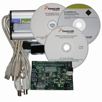
BOARD EVAL FOR MC56F8037
Manufacturer
Freescale Semiconductor
Type
MCUr
Datasheet
1.MC56F8037EVM.pdf
(180 pages)
Specifications of MC56F8037EVM
Contents
Board, Cables, CD, Debugger
Silicon Manufacturer
Freescale
Core Architecture
56800/E
Core Sub-architecture
56800/E
Silicon Core Number
MC56F
Silicon Family Name
MC56F80xx
Kit Contents
MC56F8037EVM, USB-JTAG Adapter, Cables, CD
Rohs Compliant
Yes
For Use With/related Products
MC56F8037
Lead Free Status / RoHS Status
Lead free / RoHS Compliant
Available stocks
Company
Part Number
Manufacturer
Quantity
Price
Company:

Part Number:
MC56F8037EVM
Manufacturer:
Freescale Semiconductor
Quantity:
135


6.3.6
This register controls the Standby mode of the large on-chip regulator. The large on-chip regulator derives
the core digital logic power supply from the IO power supply. At a system bus frequency of 200kHz, the
large regulator may be put in a reduced-power standby mode without interfering with device operation to
reduce device power consumption. Refer to the overview of power-down modes and the overview of clock
generation for more information on the use of large regulator standby.
6.3.6.1
This bit field is reserved. Each bit must be set to 0.
6.3.6.2
6.3.7
The Clock Output Select register can be used to multiplex out selected clock sources generated inside the
clock generation and SIM modules onto the muxed clock output pins. All functionality is for test purposes
only. Glitches may be produced when the clock is enabled or switched. The delay from the clock source
to the output is unspecified. The observability of the CLKO clock output signal at an output pad is subject
to the frequency limitations of the associated IO cell.
GPIOA[3:0] can function as GPIO, PWM, or as clock output pins. If GPIOA[3:0] are programmed to
operate as peripheral outputs, then the choice is between PWM and clock outputs. The default state is for
the peripheral function of GPIOA[3:0] to be programmed as PWM (selected by bits [9:6] of the Clock
Output Select register).
GPIOB4 can function as GPIO, or as other peripheral outputs, including clock output (CLKO). If GPIOB4
is programmed to operate as a peripheral output and CLKO is selected in the SIM_GPSB0 register, bits
[4:0] decide if CLKO is enabled or disabled and which clock source is selected if CLKO is enabled. See
Figure 6-8
100
•
•
•
•
Base + $8
RESET
00 = Large regulator is in Normal mode
01 = Large regulator is in Standby (reduced-power) mode
10 = Large regulator is in Normal mode and the LRSTDBY field is write-protected until the next reset
11 = Large regulator is in Standby mode and the LRSTDBY field is write-protected until the next reset
Read
Write
SIM Power Control Register (SIM_PWR)
Clock Output Select Register (SIM_CLKOUT)
for details.
Reserved—Bits 15–2
Large Regulator Standby Mode[1:0] (LRSTDBY)—Bits 1–0
15
0
0
Figure 6-7 SIM Power Control Register (SIM_PWR)
14
0
0
13
0
0
12
0
0
56F8037/56F8027 Data Sheet, Rev. 7
11
0
0
10
0
0
9
0
0
8
0
0
7
0
0
6
0
0
5
0
0
4
0
0
3
0
0
Freescale Semiconductor
2
0
0
1
0
LRSTDBY
0
0
Related parts for MC56F8037EVM
Image
Part Number
Description
Manufacturer
Datasheet
Request
R

Part Number:
Description:
Manufacturer:
Freescale Semiconductor, Inc
Datasheet:
Part Number:
Description:
Manufacturer:
Freescale Semiconductor, Inc
Datasheet:
Part Number:
Description:
Manufacturer:
Freescale Semiconductor, Inc
Datasheet:
Part Number:
Description:
Manufacturer:
Freescale Semiconductor, Inc
Datasheet:
Part Number:
Description:
Manufacturer:
Freescale Semiconductor, Inc
Datasheet:
Part Number:
Description:
Manufacturer:
Freescale Semiconductor, Inc
Datasheet:
Part Number:
Description:
Manufacturer:
Freescale Semiconductor, Inc
Datasheet:
Part Number:
Description:
Manufacturer:
Freescale Semiconductor, Inc
Datasheet:
Part Number:
Description:
Manufacturer:
Freescale Semiconductor, Inc
Datasheet:
Part Number:
Description:
Manufacturer:
Freescale Semiconductor, Inc
Datasheet:
Part Number:
Description:
Manufacturer:
Freescale Semiconductor, Inc
Datasheet:
Part Number:
Description:
Manufacturer:
Freescale Semiconductor, Inc
Datasheet:
Part Number:
Description:
Manufacturer:
Freescale Semiconductor, Inc
Datasheet:
Part Number:
Description:
Manufacturer:
Freescale Semiconductor, Inc
Datasheet:
Part Number:
Description:
Manufacturer:
Freescale Semiconductor, Inc
Datasheet: