MC56F8037EVM Freescale Semiconductor, MC56F8037EVM Datasheet - Page 119
MC56F8037EVM
Manufacturer Part Number
MC56F8037EVM
Description
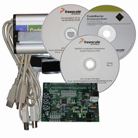
BOARD EVAL FOR MC56F8037
Manufacturer
Freescale Semiconductor
Type
MCUr
Datasheet
1.MC56F8037EVM.pdf
(180 pages)
Specifications of MC56F8037EVM
Contents
Board, Cables, CD, Debugger
Silicon Manufacturer
Freescale
Core Architecture
56800/E
Core Sub-architecture
56800/E
Silicon Core Number
MC56F
Silicon Family Name
MC56F80xx
Kit Contents
MC56F8037EVM, USB-JTAG Adapter, Cables, CD
Rohs Compliant
Yes
For Use With/related Products
MC56F8037
Lead Free Status / RoHS Status
Lead free / RoHS Compliant
Available stocks
Company
Part Number
Manufacturer
Quantity
Price
Company:

Part Number:
MC56F8037EVM
Manufacturer:
Freescale Semiconductor
Quantity:
135


6.3.20.2
This field selects the alternate function for GPIOD5.
6.3.20.3
This bit field is reserved. Each bit must be set to 0.
6.3.20.4
This field selects the alternate function for GPIOC12.
6.3.20.5
This bit field is reserved. It must be set to 0.
6.3.20.6
This field selects the alternate function for GPIOC8.
6.3.20.7
This bit field is reserved. Each bit must be set to 0.
6.3.21
The internal integration of peripherals provides input signal source selection for peripherals where an input
signal to a peripheral can be fed from one of several sources. These registers are organized by peripheral
type and provide a selection list for every peripheral input signal that has more than one alternative source
to indicate which source is selected.
If one of the alternative sources is GPIO, the setting in these registers must be made consistently with the
settings in the GPSn and GPIOx_PEREN registers. Specifically, when an IPSn field is configured to select
an I/O pin as the source, then GPSn register settings must configure only one I/O pin to feed this peripheral
input function. Also, the GPIOx_PEREN bit for that I/O pin must be set to 1 to enable peripheral control
of the I/O.
Freescale Semiconductor
•
•
•
•
•
•
0 = XTAL - External Crystal Oscillator Output (default)
1 = CLKIN - External Clock Input
0 = ANB4 - ADCB, Channel 4 (default)
1 = RXD1 - QSCI1 Receive Data
0 = ANA4 - ADCA, Channel 4 (default)
1 = TXD1 - QSCI1 Transmit Data
Internal Peripheral Source Select Register 0 for Pulse Width
Modulator (SIM_IPS0)
Configure GPIOD5 (GPS_D5)—Bit 12
Reserved—Bits 11–5
Configure GPIOC12 (GPS_C12)—Bit 4
Reserved—Bit 3
Configure GPIOC8 (GPS_C8)—Bit 2
Reserved—Bits 1—0
56F8037/56F8027 Data Sheet, Rev. 7
Register Descriptions
119
Related parts for MC56F8037EVM
Image
Part Number
Description
Manufacturer
Datasheet
Request
R

Part Number:
Description:
Manufacturer:
Freescale Semiconductor, Inc
Datasheet:
Part Number:
Description:
Manufacturer:
Freescale Semiconductor, Inc
Datasheet:
Part Number:
Description:
Manufacturer:
Freescale Semiconductor, Inc
Datasheet:
Part Number:
Description:
Manufacturer:
Freescale Semiconductor, Inc
Datasheet:
Part Number:
Description:
Manufacturer:
Freescale Semiconductor, Inc
Datasheet:
Part Number:
Description:
Manufacturer:
Freescale Semiconductor, Inc
Datasheet:
Part Number:
Description:
Manufacturer:
Freescale Semiconductor, Inc
Datasheet:
Part Number:
Description:
Manufacturer:
Freescale Semiconductor, Inc
Datasheet:
Part Number:
Description:
Manufacturer:
Freescale Semiconductor, Inc
Datasheet:
Part Number:
Description:
Manufacturer:
Freescale Semiconductor, Inc
Datasheet:
Part Number:
Description:
Manufacturer:
Freescale Semiconductor, Inc
Datasheet:
Part Number:
Description:
Manufacturer:
Freescale Semiconductor, Inc
Datasheet:
Part Number:
Description:
Manufacturer:
Freescale Semiconductor, Inc
Datasheet:
Part Number:
Description:
Manufacturer:
Freescale Semiconductor, Inc
Datasheet:
Part Number:
Description:
Manufacturer:
Freescale Semiconductor, Inc
Datasheet: