MC56F8037EVM Freescale Semiconductor, MC56F8037EVM Datasheet - Page 163
MC56F8037EVM
Manufacturer Part Number
MC56F8037EVM
Description
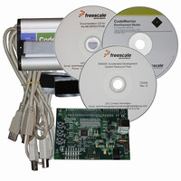
BOARD EVAL FOR MC56F8037
Manufacturer
Freescale Semiconductor
Type
MCUr
Datasheet
1.MC56F8037EVM.pdf
(180 pages)
Specifications of MC56F8037EVM
Contents
Board, Cables, CD, Debugger
Silicon Manufacturer
Freescale
Core Architecture
56800/E
Core Sub-architecture
56800/E
Silicon Core Number
MC56F
Silicon Family Name
MC56F80xx
Kit Contents
MC56F8037EVM, USB-JTAG Adapter, Cables, CD
Rohs Compliant
Yes
For Use With/related Products
MC56F8037
Lead Free Status / RoHS Status
Lead free / RoHS Compliant
Available stocks
Company
Part Number
Manufacturer
Quantity
Price
Company:

Part Number:
MC56F8037EVM
Manufacturer:
Freescale Semiconductor
Quantity:
135


10.16 Equivalent Circuit for ADC Inputs
Figure 10-18
at the same time that S3 is closed/open. When S1/S2 are closed and S3 is open, one input of the sample
and hold circuit moves to (V
the switches are flipped, the charge on C1 and C2 are averaged via S3, with the result that a single-ended
analog input is switched to a differential voltage centered about (V
switch on every cycle of the ADC clock (open one-half ADC clock, closed one-half ADC clock). Note that
there are additional capacitances associated with the analog input pad, routing, etc., but these do not filter
into the S/H output voltage, as S1 provides isolation during the charge-sharing phase.
One aspect of this circuit is that there is an on-going input current, which is a function of the analog input
voltage, V
10.17 Comparator (CMP) Parameters
Freescale Semiconductor
1. No guaranteed specification within 0.1V of V
Input Offset Voltage
Input Propagation Delay
Power-up time
1.
2.
3.
4.
Analog Input
Parasitic capacitance due to package, pin-to-pin and pin-to-package base coupling; 1.8pF
Parasitic capacitance due to the chip bond pad, ESD protection devices and signal routing; 2.04pF
Equivalent resistance for the channel select mux; 100 ohms
Sampling capacitor at the sample and hold circuit. Capacitor C1 is normally disconnected from the input and is only
connected to it at sampling time; 1.4pF
Parameter
REF
illustrates the ADC input circuit during sample and hold. S1 and S2 are always open/closed
, and the ADC clock frequency.
1
1
Figure 10-18 Equivalent Circuit for A/D Loading
Within range of V
REFHx
2
Conditions/Comments
V
- V
Table 10-21 CMP Parameters
SSA
56F8037/56F8027 Data Sheet, Rev. 7
REFLx
DDA
+ .1V
125 ESD Resistor
DDA
or V
(V
) / 2, while the other charges to the analog input voltage. When
REFHx
SSA
- .1V to
3
- V
REFLx
) / 2
V
Symbol
OFFSET
t
t
CPU
PD
8pF noise damping capacitor
S1
S2
Min
—
—
—
REFHx
4
S3
- V
C2
C1
TBD
Typ
±10
35
REFLx
Equivalent Circuit for ADC Inputs
S/H
) / 2. The switches
C1 = C2 = 1pF
Max
TBD
±35
45
Unit
mV
ns
163
Related parts for MC56F8037EVM
Image
Part Number
Description
Manufacturer
Datasheet
Request
R

Part Number:
Description:
Manufacturer:
Freescale Semiconductor, Inc
Datasheet:
Part Number:
Description:
Manufacturer:
Freescale Semiconductor, Inc
Datasheet:
Part Number:
Description:
Manufacturer:
Freescale Semiconductor, Inc
Datasheet:
Part Number:
Description:
Manufacturer:
Freescale Semiconductor, Inc
Datasheet:
Part Number:
Description:
Manufacturer:
Freescale Semiconductor, Inc
Datasheet:
Part Number:
Description:
Manufacturer:
Freescale Semiconductor, Inc
Datasheet:
Part Number:
Description:
Manufacturer:
Freescale Semiconductor, Inc
Datasheet:
Part Number:
Description:
Manufacturer:
Freescale Semiconductor, Inc
Datasheet:
Part Number:
Description:
Manufacturer:
Freescale Semiconductor, Inc
Datasheet:
Part Number:
Description:
Manufacturer:
Freescale Semiconductor, Inc
Datasheet:
Part Number:
Description:
Manufacturer:
Freescale Semiconductor, Inc
Datasheet:
Part Number:
Description:
Manufacturer:
Freescale Semiconductor, Inc
Datasheet:
Part Number:
Description:
Manufacturer:
Freescale Semiconductor, Inc
Datasheet:
Part Number:
Description:
Manufacturer:
Freescale Semiconductor, Inc
Datasheet:
Part Number:
Description:
Manufacturer:
Freescale Semiconductor, Inc
Datasheet: