MPC8313E-RDB Freescale Semiconductor, MPC8313E-RDB Datasheet - Page 14
MPC8313E-RDB
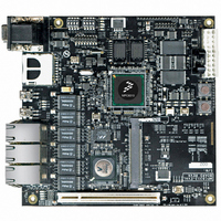
Manufacturer Part Number
MPC8313E-RDB
Description
BOARD PROCESSOR
Manufacturer
Freescale Semiconductor
Series
PowerQUICC II™ PROr
Type
MCUr
Datasheets
1.MPC8313CZQAFFB.pdf
(100 pages)
2.MPC8313E-RDBB.pdf
(52 pages)
3.MPC8313E-RDBB.pdf
(2 pages)
Specifications of MPC8313E-RDB
Contents
Reference Design Board, Software and Documentation
Termination Type
SMD
Supply Voltage Max
1.05V
Tool / Board Applications
Wired Connectivity-LIN, CAN, Ethernet, USB
Mcu Supported Families
POWERQUICC II PRO
Rohs Compliant
Yes
Filter Terminals
SMD
Silicon Manufacturer
Freescale
Silicon Core Number
MPC83xx
Kit Application Type
Communication & Networking
Application Sub Type
Ethernet
Core Architecture
Power Architecture
Silicon Family Name
PowerQUICC II PRO
For Use With/related Products
MPC8313E
Lead Free Status / RoHS Status
Lead free / RoHS Compliant


DDR and DDR2 SDRAM
Table 11
6
This section describes the DC and AC electrical specifications for the DDR SDRAM interface. Note that
DDR SDRAM is GV
6.1
Table 12
GV
14
Time for the device to turn on POR configuration signal drivers with respect to
the negation of HRESET
Notes:
1. t
2. t
3. POR configuration signals consists of CFG_RESET_SOURCE[0:2] and CFG_CLKIN_DIV.
PLL lock times
I/O supply voltage
I/O reference voltage
I/O termination voltage
Input high voltage
Input low voltage
Output leakage current
Output high current (V
Output low current (V
Notes:
1. GV
2. MV
3. V
4. Output leakage is measured with all outputs disabled, 0 V
clock is applied to the SYS_CLK_IN input, and PCI_SYNC_IN period depends on the value of CFG_CLKIN_DIV.
noise on MV
equal to MV
PCI_SYNC_IN
SYS_CLK_IN
DD
TT
DD
REF
is not applied directly to the device. It is the supply to which far end signal termination is made and is expected to be
(typ) = 1.8 V
DDR and DDR2 SDRAM
is expected to be within 50 mV of the DRAM GV
is expected to be equal to 0.5 × GV
provides the PLL lock times.
provides the recommended operating conditions for the DDR2 SDRAM component(s) when
Parameter/Condition
DDR and DDR2 SDRAM DC Electrical Characteristics
is the clock period of the input clock applied to SYS_CLK_IN. It is only valid when the device is in PCI host mode.
REF
is the clock period of the input clock applied to PCI_SYNC_IN. When the device is In PCI host mode the primary
REF
Table 12. DDR2 SDRAM DC Electrical Characteristics for GV
. This rail should track variations in the DC level of MV
may not exceed ±2% of the DC value.
OUT
OUT
MPC8313E PowerQUICC
Parameter/Condition
.
Table 10. RESET Initialization Timing Specifications (continued)
DD
= 0.280 V)
= 1.420 V)
Parameter/Condition
(typ) = 2.5 V and DDR2 SDRAM is GV
DD
Table 11. PLL Lock Times
, and to track GV
™
Symbol
MV
GV
V
II Pro Processor Hardware Specifications, Rev. 3
V
I
I
V
I
OH
OZ
OL
TT
REF
IH
IL
DD
DD
at all times.
≤
V
MV
OUT
MV
DD
0.49 × GV
REF
DC variations as measured at the receiver. Peak-to-peak
REF
≤
–13.4
–0.3
–9.9
13.4
Min
1.7
GV
+ 0.125
– 0.04
REF
DD
Min
DD
.
—
.
DD
Min
(typ) = 1.8 V.
1
MV
MV
0.51 × GV
GV
REF
DD
REF
DD
Max
Max
1.9
9.9
—
—
—
(typ) = 1.8 V
Max
100
– 0.125
+ 0.04
+ 0.3
DD
Freescale Semiconductor
t
PCI_SYNC_IN
Unit
Unit
Unit
mA
mA
μA
μs
V
V
V
V
V
Notes
Notes
Notes
1, 3
—
—
—
—
—
2
1
3
4
Related parts for MPC8313E-RDB
Image
Part Number
Description
Manufacturer
Datasheet
Request
R

Part Number:
Description:
Mpc8313e Powerquicc Ii Pro Processor
Manufacturer:
Freescale Semiconductor, Inc
Datasheet:

Part Number:
Description:
BOARD CPU 8313E VER 2.1
Manufacturer:
Freescale Semiconductor
Datasheet:

Part Number:
Description:
BOARD CPU 8313E VER 2.2
Manufacturer:
Freescale Semiconductor
Datasheet:
Part Number:
Description:
Microprocessors - MPU 8313 REV2.2 PB ENC EXT
Manufacturer:
Freescale Semiconductor
Datasheet:
Part Number:
Description:
Microprocessors - MPU 8313 REV2.2 PB W/ENC
Manufacturer:
Freescale Semiconductor
Datasheet:
Part Number:
Description:
Microprocessors - MPU 8313 REV2.2 PB NO EN EXT
Manufacturer:
Freescale Semiconductor
Datasheet:
Part Number:
Description:
Microprocessors - MPU 8313 REV2.2 PB NO ENC
Manufacturer:
Freescale Semiconductor
Datasheet:
Part Number:
Description:
Manufacturer:
Freescale Semiconductor, Inc
Datasheet:
Part Number:
Description:
Manufacturer:
Freescale Semiconductor, Inc
Datasheet:
Part Number:
Description:
Manufacturer:
Freescale Semiconductor, Inc
Datasheet:
Part Number:
Description:
Manufacturer:
Freescale Semiconductor, Inc
Datasheet:
Part Number:
Description:
Manufacturer:
Freescale Semiconductor, Inc
Datasheet:
Part Number:
Description:
Manufacturer:
Freescale Semiconductor, Inc
Datasheet:
Part Number:
Description:
Manufacturer:
Freescale Semiconductor, Inc
Datasheet:
Part Number:
Description:
Manufacturer:
Freescale Semiconductor, Inc
Datasheet: