MPC8313E-RDB Freescale Semiconductor, MPC8313E-RDB Datasheet - Page 24
MPC8313E-RDB
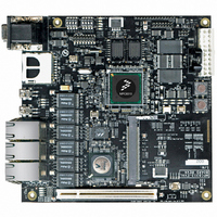
Manufacturer Part Number
MPC8313E-RDB
Description
BOARD PROCESSOR
Manufacturer
Freescale Semiconductor
Series
PowerQUICC II™ PROr
Type
MCUr
Datasheets
1.MPC8313CZQAFFB.pdf
(100 pages)
2.MPC8313E-RDBB.pdf
(52 pages)
3.MPC8313E-RDBB.pdf
(2 pages)
Specifications of MPC8313E-RDB
Contents
Reference Design Board, Software and Documentation
Termination Type
SMD
Supply Voltage Max
1.05V
Tool / Board Applications
Wired Connectivity-LIN, CAN, Ethernet, USB
Mcu Supported Families
POWERQUICC II PRO
Rohs Compliant
Yes
Filter Terminals
SMD
Silicon Manufacturer
Freescale
Silicon Core Number
MPC83xx
Kit Application Type
Communication & Networking
Application Sub Type
Ethernet
Core Architecture
Power Architecture
Silicon Family Name
PowerQUICC II PRO
For Use With/related Products
MPC8313E
Lead Free Status / RoHS Status
Lead free / RoHS Compliant


Ethernet: Three-Speed Ethernet, MII Management
Figure 9
Figure 10
24
At recommended operating conditions with LV
RXD[3:0], RX_DV, RX_ER hold time to RX_CLK
RX_CLK clock rise V
RX_CLK clock fall time V
Note:
1. The symbols used for timing specifications follow the pattern of t
inputs and t
timing (MR) with respect to the time data input signals (D) reach the valid state (V) relative to the t
going to the high (H) state or setup time. Also, t
signals (D) went invalid (X) relative to the t
the clock reference symbol representation is based on three letters representing the clock of a particular functional. For
example, the subscript of t
with the appropriate letter: R (rise) or F (fall).
provides the AC test load for TSEC.
shows the MII receive AC timing diagram.
(first two letters of functional block)(reference)(state)(signal)(state)
RXD[3:0]
RX_CLK
Parameter/Condition
Figure 10. MII Receive AC Timing Diagram RMII AC Timing Specifications
RX_DV
RX_ER
IL
Output
MPC8313E PowerQUICC
(min) to V
IH
(max) to V
Table 27. MII Receive AC Timing Specifications (continued)
MRX
IH
represents the MII (M) receive (RX) clock. For rise and fall times, the latter convention is used
(max)
IL
t
(min)
t
MRXH
MRDVKH
DDA
Z
/
MRX
LV
0
Figure 9. TSEC AC Test Load
t
= 50 Ω
MRX
DDB
clock reference (K) going to the low (L) state or hold time. Note that, in general,
™
MRDXKL
/NV
II Pro Processor Hardware Specifications, Rev. 3
DD
of 3.3 V ± 0.3 V.
Valid Data
symbolizes MII receive timing (GR) with respect to the time data input
t
Symbol
MRXF
t
MRDXKH
t
t
(first two letters of functional block)(signal)(state)(reference)(state)
MRXR
MRXF
for outputs. For example, t
R
L
1
= 50 Ω
t
MRDXKH
t
MRXR
10.0
Min
1.0
1.0
LV
DDA
/2 or LV
MRDVKH
Typ
—
—
—
DDB
MRX
Freescale Semiconductor
symbolizes MII receive
/2
clock reference (K)
Max
4.0
4.0
—
Unit
ns
ns
ns
for
Related parts for MPC8313E-RDB
Image
Part Number
Description
Manufacturer
Datasheet
Request
R

Part Number:
Description:
Mpc8313e Powerquicc Ii Pro Processor
Manufacturer:
Freescale Semiconductor, Inc
Datasheet:

Part Number:
Description:
BOARD CPU 8313E VER 2.1
Manufacturer:
Freescale Semiconductor
Datasheet:

Part Number:
Description:
BOARD CPU 8313E VER 2.2
Manufacturer:
Freescale Semiconductor
Datasheet:
Part Number:
Description:
Microprocessors - MPU 8313 REV2.2 PB ENC EXT
Manufacturer:
Freescale Semiconductor
Datasheet:
Part Number:
Description:
Microprocessors - MPU 8313 REV2.2 PB W/ENC
Manufacturer:
Freescale Semiconductor
Datasheet:
Part Number:
Description:
Microprocessors - MPU 8313 REV2.2 PB NO EN EXT
Manufacturer:
Freescale Semiconductor
Datasheet:
Part Number:
Description:
Microprocessors - MPU 8313 REV2.2 PB NO ENC
Manufacturer:
Freescale Semiconductor
Datasheet:
Part Number:
Description:
Manufacturer:
Freescale Semiconductor, Inc
Datasheet:
Part Number:
Description:
Manufacturer:
Freescale Semiconductor, Inc
Datasheet:
Part Number:
Description:
Manufacturer:
Freescale Semiconductor, Inc
Datasheet:
Part Number:
Description:
Manufacturer:
Freescale Semiconductor, Inc
Datasheet:
Part Number:
Description:
Manufacturer:
Freescale Semiconductor, Inc
Datasheet:
Part Number:
Description:
Manufacturer:
Freescale Semiconductor, Inc
Datasheet:
Part Number:
Description:
Manufacturer:
Freescale Semiconductor, Inc
Datasheet:
Part Number:
Description:
Manufacturer:
Freescale Semiconductor, Inc
Datasheet: