MPC8313E-RDB Freescale Semiconductor, MPC8313E-RDB Datasheet - Page 88
MPC8313E-RDB
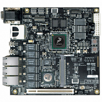
Manufacturer Part Number
MPC8313E-RDB
Description
BOARD PROCESSOR
Manufacturer
Freescale Semiconductor
Series
PowerQUICC II™ PROr
Type
MCUr
Datasheets
1.MPC8313CZQAFFB.pdf
(100 pages)
2.MPC8313E-RDBB.pdf
(52 pages)
3.MPC8313E-RDBB.pdf
(2 pages)
Specifications of MPC8313E-RDB
Contents
Reference Design Board, Software and Documentation
Termination Type
SMD
Supply Voltage Max
1.05V
Tool / Board Applications
Wired Connectivity-LIN, CAN, Ethernet, USB
Mcu Supported Families
POWERQUICC II PRO
Rohs Compliant
Yes
Filter Terminals
SMD
Silicon Manufacturer
Freescale
Silicon Core Number
MPC83xx
Kit Application Type
Communication & Networking
Application Sub Type
Ethernet
Core Architecture
Power Architecture
Silicon Family Name
PowerQUICC II PRO
For Use With/related Products
MPC8313E
Lead Free Status / RoHS Status
Lead free / RoHS Compliant


System Design Information
22 System Design Information
This section provides electrical and thermal design recommendations for successful application of the
MPC8313E SYS_CLK_IN
22.1
The MPC8313E includes three PLLs.
22.2
Each of the PLLs listed above is provided with power through independent power supply pins (AV
AV
these voltages are derived directly from V
There are a number of ways to reliably provide power to the PLLs, but the recommended solution is to
provide independent filter circuits as illustrated in
providing independent filters to each PLL the opportunity to cause noise injection from one PLL to the
other is reduced.
This circuit is intended to filter noise in the PLLs resonant frequency range from a 500 kHz to 10 MHz
range. It should be built with surface mount capacitors with minimum effective series inductance (ESL).
Consistent with the recommendations of Dr. Howard Johnson in High Speed Digital Design: A Handbook
of Black Magic (Prentice Hall, 1993), multiple small capacitors of equal value are recommended over a
single large value capacitor.
Each circuit should be placed as close as possible to the specific AV
noise coupled from nearby circuits. It should be possible to route directly from the capacitors to the AV
pin, which is on the periphery of package, without the inductance of vias.
Figure 58
88
DD2
1. The platform PLL (AV
2. The e300 core PLL (AV
3. There is a PLL for the SerDes block.
, and SDAV
SYS_CLK_IN input in PCI host mode or SYS_CLK_IN/PCI_SYNC_IN in PCI agent mode. The
frequency ratio between the platform and SYS_CLK_IN is selected using the platform PLL ratio
configuration bits as described in
frequency ratio between the e300 core clock and the platform clock is selected using the e300
PLL ratio configuration bits as described in
System Clocking
PLL Power Supply Filtering
shows the PLL power supply filter circuits.
DD
MPC8313E PowerQUICC
V
, respectively). The AV
DD
DD2
DD1
Figure 58. PLL Power Supply Filter Circuit
1.0 Ω
)
generates the platform clock from the externally supplied
)
generates the core clock as a slave to the platform clock. The
™
Section 20.1, “System PLL
2.2 µF
DD
II Pro Processor Hardware Specifications, Rev. 3
DD
through a low frequency filter scheme such as the following.
level should always be equivalent to V
Figure
Section 20.2, “Core PLL Configuration.”
Low ESL Surface Mount Capacitors
2.2 µF
58, one to each of the five AV
AV
DD
Configuration.”
DD1
pin being supplied to minimize
and AV
DD2
Freescale Semiconductor
DD
DD
, and preferably
pins. By
DD1
DD
,
Related parts for MPC8313E-RDB
Image
Part Number
Description
Manufacturer
Datasheet
Request
R

Part Number:
Description:
Mpc8313e Powerquicc Ii Pro Processor
Manufacturer:
Freescale Semiconductor, Inc
Datasheet:

Part Number:
Description:
BOARD CPU 8313E VER 2.1
Manufacturer:
Freescale Semiconductor
Datasheet:

Part Number:
Description:
BOARD CPU 8313E VER 2.2
Manufacturer:
Freescale Semiconductor
Datasheet:
Part Number:
Description:
Microprocessors - MPU 8313 REV2.2 PB ENC EXT
Manufacturer:
Freescale Semiconductor
Datasheet:
Part Number:
Description:
Microprocessors - MPU 8313 REV2.2 PB W/ENC
Manufacturer:
Freescale Semiconductor
Datasheet:
Part Number:
Description:
Microprocessors - MPU 8313 REV2.2 PB NO EN EXT
Manufacturer:
Freescale Semiconductor
Datasheet:
Part Number:
Description:
Microprocessors - MPU 8313 REV2.2 PB NO ENC
Manufacturer:
Freescale Semiconductor
Datasheet:
Part Number:
Description:
Manufacturer:
Freescale Semiconductor, Inc
Datasheet:
Part Number:
Description:
Manufacturer:
Freescale Semiconductor, Inc
Datasheet:
Part Number:
Description:
Manufacturer:
Freescale Semiconductor, Inc
Datasheet:
Part Number:
Description:
Manufacturer:
Freescale Semiconductor, Inc
Datasheet:
Part Number:
Description:
Manufacturer:
Freescale Semiconductor, Inc
Datasheet:
Part Number:
Description:
Manufacturer:
Freescale Semiconductor, Inc
Datasheet:
Part Number:
Description:
Manufacturer:
Freescale Semiconductor, Inc
Datasheet:
Part Number:
Description:
Manufacturer:
Freescale Semiconductor, Inc
Datasheet: