MPC8313E-RDB Freescale Semiconductor, MPC8313E-RDB Datasheet - Page 17
MPC8313E-RDB
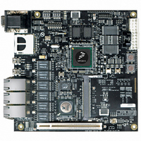
Manufacturer Part Number
MPC8313E-RDB
Description
BOARD PROCESSOR
Manufacturer
Freescale Semiconductor
Series
PowerQUICC II™ PROr
Type
MCUr
Datasheets
1.MPC8313CZQAFFB.pdf
(100 pages)
2.MPC8313E-RDBB.pdf
(52 pages)
3.MPC8313E-RDBB.pdf
(2 pages)
Specifications of MPC8313E-RDB
Contents
Reference Design Board, Software and Documentation
Termination Type
SMD
Supply Voltage Max
1.05V
Tool / Board Applications
Wired Connectivity-LIN, CAN, Ethernet, USB
Mcu Supported Families
POWERQUICC II PRO
Rohs Compliant
Yes
Filter Terminals
SMD
Silicon Manufacturer
Freescale
Silicon Core Number
MPC83xx
Kit Application Type
Communication & Networking
Application Sub Type
Ethernet
Core Architecture
Power Architecture
Silicon Family Name
PowerQUICC II PRO
For Use With/related Products
MPC8313E
Lead Free Status / RoHS Status
Lead free / RoHS Compliant


Figure 4
6.2.2
Freescale Semiconductor
MCK[ n ] cycle time, MCK[ n ]/MCK[ n ] crossing
ADDR/CMD output setup with respect to MCK
ADDR/CMD output hold with respect to MCK
MCS[ n ] output setup with respect to MCK
MCS[ n ] output hold with respect to MCK
MCK to MDQS Skew
MDQ//MDM output setup with respect to
MDQS
MDQ//MDM output hold with respect to MDQS
MDQS preamble start
illustrates the DDR input timing diagram showing the t
Table 20. DDR and DDR2 SDRAM Output AC Timing Specifications for Rev. 1.0 Silicon
MDQS[ n ]
DDR and DDR2 SDRAM Output AC Timing Specifications
MDQ[ x ]
MCK[ n ]
MCK[ n ]
Parameter
MPC8313E PowerQUICC
333 MHz
266 MHz
333 MHz
266 MHz
333 MHz
266 MHz
333 MHz
266 MHz
333 MHz
266 MHz
333 MHz
266 MHz
t
t
MCK
Figure 4. DDR Input Timing Diagram
DISKEW
™
Symbol
t
t
t
t
t
t
t
t
t
t
DDKHMH
DDKHDS,
DDKHDX,
DDKHMP
DDKHAS
DDKHAX
DDKHCS
DDKHCX
DDKLDS
DDKLDX
II Pro Processor Hardware Specifications, Rev. 3
t
MCK
D0
1
–0.5 × t
D1
t
DISKEW
3.15
–0.6
1100
Min
3.15
3.15
800
900
900
2.1
2.5
2.4
2.4
2.4
MCK
6
– 0.6
DISKEW
–0.5 × t
timing parameter.
Max
0.6
10
—
—
—
—
—
—
—
—
—
—
—
—
MCK
+ 0.6
DDR and DDR2 SDRAM
Unit
ns
ns
ns
ns
ns
ns
ps
ps
ns
Notes
2
4
6
3
3
3
3
5
5
17
Related parts for MPC8313E-RDB
Image
Part Number
Description
Manufacturer
Datasheet
Request
R

Part Number:
Description:
Mpc8313e Powerquicc Ii Pro Processor
Manufacturer:
Freescale Semiconductor, Inc
Datasheet:

Part Number:
Description:
BOARD CPU 8313E VER 2.1
Manufacturer:
Freescale Semiconductor
Datasheet:

Part Number:
Description:
BOARD CPU 8313E VER 2.2
Manufacturer:
Freescale Semiconductor
Datasheet:
Part Number:
Description:
Microprocessors - MPU 8313 REV2.2 PB ENC EXT
Manufacturer:
Freescale Semiconductor
Datasheet:
Part Number:
Description:
Microprocessors - MPU 8313 REV2.2 PB W/ENC
Manufacturer:
Freescale Semiconductor
Datasheet:
Part Number:
Description:
Microprocessors - MPU 8313 REV2.2 PB NO EN EXT
Manufacturer:
Freescale Semiconductor
Datasheet:
Part Number:
Description:
Microprocessors - MPU 8313 REV2.2 PB NO ENC
Manufacturer:
Freescale Semiconductor
Datasheet:
Part Number:
Description:
Manufacturer:
Freescale Semiconductor, Inc
Datasheet:
Part Number:
Description:
Manufacturer:
Freescale Semiconductor, Inc
Datasheet:
Part Number:
Description:
Manufacturer:
Freescale Semiconductor, Inc
Datasheet:
Part Number:
Description:
Manufacturer:
Freescale Semiconductor, Inc
Datasheet:
Part Number:
Description:
Manufacturer:
Freescale Semiconductor, Inc
Datasheet:
Part Number:
Description:
Manufacturer:
Freescale Semiconductor, Inc
Datasheet:
Part Number:
Description:
Manufacturer:
Freescale Semiconductor, Inc
Datasheet:
Part Number:
Description:
Manufacturer:
Freescale Semiconductor, Inc
Datasheet: