MPC8313E-RDB Freescale Semiconductor, MPC8313E-RDB Datasheet - Page 41
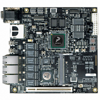
MPC8313E-RDB
Manufacturer Part Number
MPC8313E-RDB
Description
BOARD PROCESSOR
Manufacturer
Freescale Semiconductor
Series
PowerQUICC II™ PROr
Type
MCUr
Datasheets
1.MPC8313CZQAFFB.pdf
(100 pages)
2.MPC8313E-RDBB.pdf
(52 pages)
3.MPC8313E-RDBB.pdf
(2 pages)
Specifications of MPC8313E-RDB
Contents
Reference Design Board, Software and Documentation
Termination Type
SMD
Supply Voltage Max
1.05V
Tool / Board Applications
Wired Connectivity-LIN, CAN, Ethernet, USB
Mcu Supported Families
POWERQUICC II PRO
Rohs Compliant
Yes
Filter Terminals
SMD
Silicon Manufacturer
Freescale
Silicon Core Number
MPC83xx
Kit Application Type
Communication & Networking
Application Sub Type
Ethernet
Core Architecture
Power Architecture
Silicon Family Name
PowerQUICC II PRO
For Use With/related Products
MPC8313E
Lead Free Status / RoHS Status
Lead free / RoHS Compliant


Figure 27
assumes that the DC levels of the clock driver chip is compatible with MPC8313E SerDes reference clock
input’s DC requirement.
Figure 28
Since LVDS clock driver’s common mode voltage is higher than the MPC8313E SerDes reference clock
input’s allowed range (100 to 400 mV), the AC-coupled connection scheme must be used. It assumes the
LVDS output driver features a 50-Ω termination resistor. It also assumes that the LVDS transmitter
establishes its own common mode level without relying on the receiver or other external component.
Freescale Semiconductor
HCSL CLK Driver Chip
Total 50 Ω. Assume clock driver’s
output impedance is about 16 Ω.
Clock Driver
Clock Driver
Figure 27. DC-Coupled Differential Connection with HCSL Clock Driver (Reference Only)
shows the SerDes reference clock connection reference circuits for HCSL type clock driver. It
shows the SerDes reference clock connection reference circuits for LVDS type clock driver.
CLK_Out
CLK_Out
Figure 27
fact that the clock driver chip's internal structure, output impedance, and
termination requirements are different between various clock driver chip
manufacturers, it is possible that the clock circuit reference designs
provided by clock driver chip vendors are different from what is shown in
the figures. They might also vary from one vendor to the other. Therefore,
Freescale can neither provide the optimal clock driver reference circuits, nor
guarantee the correctness of the following clock driver connection reference
circuits. It is recommended that the system designer contact the selected
clock driver chip vendor for the optimal reference circuits for the
MPC8313E SerDes reference clock receiver requirement provided in this
document.
MPC8313E PowerQUICC
through
33 Ω
33 Ω
Figure 30
Clock driver vendor dependent
source termination resistor
100 Ω Differential PWB Trace
™
II Pro Processor Hardware Specifications, Rev. 3
are for conceptual reference only. Due to the
NOTE
SD n _REF_CLK
SD n _REF_CLK
SDn_REF_CLK
50 Ω
50 Ω
High-Speed Serial Interfaces (HSSI)
MPC8313E
SerDes Refer.
CLK Receiver
41
Related parts for MPC8313E-RDB
Image
Part Number
Description
Manufacturer
Datasheet
Request
R

Part Number:
Description:
Mpc8313e Powerquicc Ii Pro Processor
Manufacturer:
Freescale Semiconductor, Inc
Datasheet:

Part Number:
Description:
BOARD CPU 8313E VER 2.1
Manufacturer:
Freescale Semiconductor
Datasheet:

Part Number:
Description:
BOARD CPU 8313E VER 2.2
Manufacturer:
Freescale Semiconductor
Datasheet:
Part Number:
Description:
Microprocessors - MPU 8313 REV2.2 PB ENC EXT
Manufacturer:
Freescale Semiconductor
Datasheet:
Part Number:
Description:
Microprocessors - MPU 8313 REV2.2 PB W/ENC
Manufacturer:
Freescale Semiconductor
Datasheet:
Part Number:
Description:
Microprocessors - MPU 8313 REV2.2 PB NO EN EXT
Manufacturer:
Freescale Semiconductor
Datasheet:
Part Number:
Description:
Microprocessors - MPU 8313 REV2.2 PB NO ENC
Manufacturer:
Freescale Semiconductor
Datasheet:
Part Number:
Description:
Manufacturer:
Freescale Semiconductor, Inc
Datasheet:
Part Number:
Description:
Manufacturer:
Freescale Semiconductor, Inc
Datasheet:
Part Number:
Description:
Manufacturer:
Freescale Semiconductor, Inc
Datasheet:
Part Number:
Description:
Manufacturer:
Freescale Semiconductor, Inc
Datasheet:
Part Number:
Description:
Manufacturer:
Freescale Semiconductor, Inc
Datasheet:
Part Number:
Description:
Manufacturer:
Freescale Semiconductor, Inc
Datasheet:
Part Number:
Description:
Manufacturer:
Freescale Semiconductor, Inc
Datasheet:
Part Number:
Description:
Manufacturer:
Freescale Semiconductor, Inc
Datasheet: