MPC8313E-RDB Freescale Semiconductor, MPC8313E-RDB Datasheet - Page 9
MPC8313E-RDB
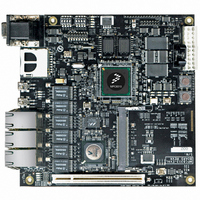
Manufacturer Part Number
MPC8313E-RDB
Description
BOARD PROCESSOR
Manufacturer
Freescale Semiconductor
Series
PowerQUICC II™ PROr
Type
MCUr
Datasheets
1.MPC8313CZQAFFB.pdf
(100 pages)
2.MPC8313E-RDBB.pdf
(52 pages)
3.MPC8313E-RDBB.pdf
(2 pages)
Specifications of MPC8313E-RDB
Contents
Reference Design Board, Software and Documentation
Termination Type
SMD
Supply Voltage Max
1.05V
Tool / Board Applications
Wired Connectivity-LIN, CAN, Ethernet, USB
Mcu Supported Families
POWERQUICC II PRO
Rohs Compliant
Yes
Filter Terminals
SMD
Silicon Manufacturer
Freescale
Silicon Core Number
MPC83xx
Kit Application Type
Communication & Networking
Application Sub Type
Ethernet
Core Architecture
Power Architecture
Silicon Family Name
PowerQUICC II PRO
For Use With/related Products
MPC8313E
Lead Free Status / RoHS Status
Lead free / RoHS Compliant


Figure 2
2.1.3
Table 3
2.2
The MPC8313E does not require the core supply voltage (V
LV
supplies are stable and if the I/O voltages are supplied before the core voltage, there might be a period of
time that all input and output pins are actively driven and cause contention and excessive current. In order
to avoid actively driving the I/O pins and to eliminate excessive current draw, apply the core voltage (V
Freescale Semiconductor
DD
, and OV
provides information on the characteristics of the output driver strengths.
shows the undershoot and overshoot voltages at the interfaces of the MPC8313E.
Power Sequencing
Local bus interface utilities signals
PCI signals
DDR signal
DDR2 signal
DUART, system control, I
GPIO signals
eTSEC signals
USB signals
Output Driver Characteristics
DD
) to be applied in any particular order. Note that during power ramp-up, before the power
V
V
Note:
MPC8313E PowerQUICC
IH
1. Note that t
IL
interface.
Figure 2. Overshoot/Undershoot Voltage for GV
Driver Type
G/L/NV
G/L/NV
V
V
SS
SS
G/L/NV
DD
interface
DD
– 0.3 V
– 0.7 V
2
+ 20%
C, JTAG, SPI
+ 5%
V
DD
SS
refers to the clock period associated with the bus clock
Table 3. Output Drive Capability
™
II Pro Processor Hardware Specifications, Rev. 3
Output Impedance (Ω)
Not to Exceed 10%
42
25
18
18
42
42
42
42
of t
DD
interface
and V
1
DDC
DD
/NV
LV
) and IO supply voltages (GV
DDA
DD
LV
Supply Voltage
NV
GV
GV
NV
NV
, LV
/LV
DDB
DD
DD
DD
DD
DD
DD
DDB
= 2.5/3.3 V
= 3.3 V
= 3.3 V
= 3.3 V
= 2.5 V
= 1.8 V
= 2.5/3.3 V
Electrical Characteristics
DD
DD
,
9
Related parts for MPC8313E-RDB
Image
Part Number
Description
Manufacturer
Datasheet
Request
R

Part Number:
Description:
Mpc8313e Powerquicc Ii Pro Processor
Manufacturer:
Freescale Semiconductor, Inc
Datasheet:

Part Number:
Description:
BOARD CPU 8313E VER 2.1
Manufacturer:
Freescale Semiconductor
Datasheet:

Part Number:
Description:
BOARD CPU 8313E VER 2.2
Manufacturer:
Freescale Semiconductor
Datasheet:
Part Number:
Description:
Microprocessors - MPU 8313 REV2.2 PB ENC EXT
Manufacturer:
Freescale Semiconductor
Datasheet:
Part Number:
Description:
Microprocessors - MPU 8313 REV2.2 PB W/ENC
Manufacturer:
Freescale Semiconductor
Datasheet:
Part Number:
Description:
Microprocessors - MPU 8313 REV2.2 PB NO EN EXT
Manufacturer:
Freescale Semiconductor
Datasheet:
Part Number:
Description:
Microprocessors - MPU 8313 REV2.2 PB NO ENC
Manufacturer:
Freescale Semiconductor
Datasheet:
Part Number:
Description:
Manufacturer:
Freescale Semiconductor, Inc
Datasheet:
Part Number:
Description:
Manufacturer:
Freescale Semiconductor, Inc
Datasheet:
Part Number:
Description:
Manufacturer:
Freescale Semiconductor, Inc
Datasheet:
Part Number:
Description:
Manufacturer:
Freescale Semiconductor, Inc
Datasheet:
Part Number:
Description:
Manufacturer:
Freescale Semiconductor, Inc
Datasheet:
Part Number:
Description:
Manufacturer:
Freescale Semiconductor, Inc
Datasheet:
Part Number:
Description:
Manufacturer:
Freescale Semiconductor, Inc
Datasheet:
Part Number:
Description:
Manufacturer:
Freescale Semiconductor, Inc
Datasheet: