MPC8360E-RDK Freescale Semiconductor, MPC8360E-RDK Datasheet - Page 16
MPC8360E-RDK
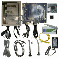
Manufacturer Part Number
MPC8360E-RDK
Description
BOARD REFERENCE DESIGN FOR MPC
Manufacturer
Freescale Semiconductor
Series
PowerQUICC II™ PROr
Type
MPUr
Specifications of MPC8360E-RDK
Contents
Board, Cables, CD, Power Supply
Processor To Be Evaluated
MPC8360E
Data Bus Width
32 bit
Interface Type
RS-232, Ethernet, USB
Operating Supply Voltage
1.3 V
For Use With/related Products
MPC8360E
Lead Free Status / RoHS Status
Lead free / RoHS Compliant


Clock Input Timing
4.1
Table 7
4.2
The primary clock source for the device can be one of two inputs, CLKIN or PCI_CLK, depending on
whether the device is configured in PCI host or PCI agent mode.
(CLKIN/PCI_CLK) AC timing specifications for the device.
16
Input high voltage
Input low voltage
CLKIN input current
PCI_SYNC_IN input current
PCI_SYNC_IN input current
CLKIN/PCI_CLK frequency
CLKIN/PCI_CLK cycle time
CLKIN/PCI_CLK rise and fall time
CLKIN/PCI_CLK duty cycle
CLKIN/PCI_CLK jitter
Notes:
1. Caution: The system, core, USB, security, and 10/100/1000 Ethernet must not exceed their respective maximum or minimum
2. Rise and fall times for CLKIN/PCI_CLK are measured at 0.4 V and 2.7 V.
3. Timing is guaranteed by design and characterization.
4. This represents the total input jitter—short term and long term—and is guaranteed by design.
5. The CLKIN/PCI_CLK driver’s closed loop jitter bandwidth should be <500 kHz at –20 dB. The bandwidth must be set low to
operating frequencies.
allow cascade-connected PLL-based devices to track CLKIN drivers with the specified jitter.
MPC8360E/MPC8358E PowerQUICC II Pro Processor Revision 2.x TBGA Silicon Hardware Specifications, Rev. 4
provides the clock input (CLKIN/PCI_SYNC_IN) DC timing specifications for the device.
Parameter
DC Electrical Characteristics
AC Electrical Characteristics
Parameter/Condition
Table 7. CLKIN DC Electrical Characteristics
0.5 V ≤ V
OV
Table 8. CLKIN AC Timing Specifications
DD
0 V ≤ V
0 V ≤ V
– 0.5V ≤ V
Condition
IN
IN
≤ OV
IN
—
—
≤ 0.5V or
≤ OV
t
KHK
DD
Symbol
IN
t
KH
f
t
CLKIN
CLKIN
≤ OV
DD
/t
—
– 0.5 V
, t
CLKIN
KL
DD
Min
0.6
Symbol
15
40
—
—
V
V
I
I
I
IN
IN
IN
IH
IL
Table 8
Typical
1.0
—
—
—
—
provides the clock input
–0.3
Min
2.7
—
—
—
66.67
±150
Max
2.3
60
—
Freescale Semiconductor
OV
DD
±100
Max
±10
±10
0.4
MHz
Unit
+ 0.3
ns
ns
ps
%
Notes
Unit
4, 5
μA
μA
μA
—
V
V
1
2
3
Related parts for MPC8360E-RDK
Image
Part Number
Description
Manufacturer
Datasheet
Request
R

Part Number:
Description:
Mpc8360e Powerquicc Ii Pro Family
Manufacturer:
Freescale Semiconductor, Inc
Datasheet:

Part Number:
Description:
BOARD PROCESSOR FOR MPC8360E
Manufacturer:
Freescale Semiconductor
Datasheet:
Part Number:
Description:
Manufacturer:
Freescale Semiconductor, Inc
Datasheet:
Part Number:
Description:
Manufacturer:
Freescale Semiconductor, Inc
Datasheet:
Part Number:
Description:
Manufacturer:
Freescale Semiconductor, Inc
Datasheet:
Part Number:
Description:
Manufacturer:
Freescale Semiconductor, Inc
Datasheet:
Part Number:
Description:
Manufacturer:
Freescale Semiconductor, Inc
Datasheet:
Part Number:
Description:
Manufacturer:
Freescale Semiconductor, Inc
Datasheet:
Part Number:
Description:
Manufacturer:
Freescale Semiconductor, Inc
Datasheet:
Part Number:
Description:
Manufacturer:
Freescale Semiconductor, Inc
Datasheet:
Part Number:
Description:
Manufacturer:
Freescale Semiconductor, Inc
Datasheet:
Part Number:
Description:
Manufacturer:
Freescale Semiconductor, Inc
Datasheet:
Part Number:
Description:
Manufacturer:
Freescale Semiconductor, Inc
Datasheet:
Part Number:
Description:
Manufacturer:
Freescale Semiconductor, Inc
Datasheet:
Part Number:
Description:
Manufacturer:
Freescale Semiconductor, Inc
Datasheet: