MPC8360E-RDK Freescale Semiconductor, MPC8360E-RDK Datasheet - Page 90
MPC8360E-RDK
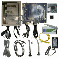
Manufacturer Part Number
MPC8360E-RDK
Description
BOARD REFERENCE DESIGN FOR MPC
Manufacturer
Freescale Semiconductor
Series
PowerQUICC II™ PROr
Type
MPUr
Specifications of MPC8360E-RDK
Contents
Board, Cables, CD, Power Supply
Processor To Be Evaluated
MPC8360E
Data Bus Width
32 bit
Interface Type
RS-232, Ethernet, USB
Operating Supply Voltage
1.3 V
For Use With/related Products
MPC8360E
Lead Free Status / RoHS Status
Lead free / RoHS Compliant


Clocking
The system VCO frequency is derived from the following equations:
As described in
configuration word low and the CFG_CLKIN_DIV configuration input signal select the ratio between the
primary clock input (CLKIN or PCI_CLK) and the internal coherent system bus clock (csb_clk).
shows the expected frequency values for the CSB frequency for select csb_clk to CLKIN/PCI_SYNC_IN
ratios.
90
MPC8360E/MPC8358E PowerQUICC II Pro Processor Revision 2.x TBGA Silicon Hardware Specifications, Rev. 4
•
•
•
CFG_CLKIN_DIV
csb_clk = {PCI_SYNC_IN × (1 + CFG_CLKIN_DIV)} × SPMF
System VCO Frequency = csb_clk × VCO divider (if both RCWL[DDRCM] and RCWL[LBCM]
are cleared)
OR
System VCO frequency = 2 × csb_clk × VCO divider (if either RCWL[DDRCM] or
RCWL[LBCM] are set).
at Reset
High
High
High
High
Low
Low
Low
Low
Low
Low
Low
Low
Low
Low
Low
Low
Low
Low
Low
1
Section 22, “Clocking,”
SPMF
0010
0011
0100
0101
0110
0111
1000
1001
1010
1011
1100
1101
1110
1111
0000
0010
0011
0100
0101
Table 72. CSB Frequency Options
the LBCM, DDRCM, and SPMF parameters in the reset
Input Clock Ratio
csb_clk :
10:1
11:1
12:1
13:1
14:1
15:1
16:1
2:1
3:1
4:1
5:1
6:1
7:1
8:1
9:1
2:1
3:1
4:1
5:1
2
100
116
133
150
166
183
200
216
16.67
233
250
266
Input Clock Frequency (MHz)
csb_clk Frequency (MHz)
100
125
150
175
200
225
250
275
300
325
25
Freescale Semiconductor
33.33
100
133
166
200
233
266
300
333
100
133
166
2
Table 72
66.67
133
200
266
333
133
200
266
333
Related parts for MPC8360E-RDK
Image
Part Number
Description
Manufacturer
Datasheet
Request
R

Part Number:
Description:
Mpc8360e Powerquicc Ii Pro Family
Manufacturer:
Freescale Semiconductor, Inc
Datasheet:

Part Number:
Description:
BOARD PROCESSOR FOR MPC8360E
Manufacturer:
Freescale Semiconductor
Datasheet:
Part Number:
Description:
Manufacturer:
Freescale Semiconductor, Inc
Datasheet:
Part Number:
Description:
Manufacturer:
Freescale Semiconductor, Inc
Datasheet:
Part Number:
Description:
Manufacturer:
Freescale Semiconductor, Inc
Datasheet:
Part Number:
Description:
Manufacturer:
Freescale Semiconductor, Inc
Datasheet:
Part Number:
Description:
Manufacturer:
Freescale Semiconductor, Inc
Datasheet:
Part Number:
Description:
Manufacturer:
Freescale Semiconductor, Inc
Datasheet:
Part Number:
Description:
Manufacturer:
Freescale Semiconductor, Inc
Datasheet:
Part Number:
Description:
Manufacturer:
Freescale Semiconductor, Inc
Datasheet:
Part Number:
Description:
Manufacturer:
Freescale Semiconductor, Inc
Datasheet:
Part Number:
Description:
Manufacturer:
Freescale Semiconductor, Inc
Datasheet:
Part Number:
Description:
Manufacturer:
Freescale Semiconductor, Inc
Datasheet:
Part Number:
Description:
Manufacturer:
Freescale Semiconductor, Inc
Datasheet:
Part Number:
Description:
Manufacturer:
Freescale Semiconductor, Inc
Datasheet: