MPC8360E-RDK Freescale Semiconductor, MPC8360E-RDK Datasheet - Page 54
MPC8360E-RDK
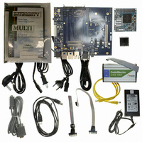
Manufacturer Part Number
MPC8360E-RDK
Description
BOARD REFERENCE DESIGN FOR MPC
Manufacturer
Freescale Semiconductor
Series
PowerQUICC II™ PROr
Type
MPUr
Specifications of MPC8360E-RDK
Contents
Board, Cables, CD, Power Supply
Processor To Be Evaluated
MPC8360E
Data Bus Width
32 bit
Interface Type
RS-232, Ethernet, USB
Operating Supply Voltage
1.3 V
For Use With/related Products
MPC8360E
Lead Free Status / RoHS Status
Lead free / RoHS Compliant


PCI
12 PCI
This section describes the DC and AC electrical specifications for the PCI bus of the MPC8360E/58E.
12.1
Table 46
12.2
This section describes the general AC timing parameters of the PCI bus of the device. Note that the
PCI_CLK or PCI_SYNC_IN signal is used as the PCI input clock depending on whether the device is
configured as a host or agent device.
54
High-level input voltage
Low-level input voltage
High-level output voltage
Low-level output voltage
Input current
Note:
1. Note that the symbol V
Clock to output valid
Output hold from clock
Clock to output high impedance
Input setup to clock
Input hold from clock
Notes:
1. The symbols used for timing specifications follow the pattern of t
2. See the timing measurement conditions in the PCI 2.2 Local Bus Specifications .
3. For purposes of active/float timing measurements, the Hi-Z or off-state is defined to be when the total current delivered
4. Input timings are measured at the pin.
5. In rev. 2.0 silicon, due to errata, t
6. In rev. 2.0 silicon, due to errata, t
.
inputs and t
(PC) with respect to the time the input signals (I) reach the valid state (V) relative to the PCI_SYNC_IN clock, t
(K) going to the high (H) state or setup time. Also, t
(R) went high (H) relative to the frame signal (F) going to the valid (V) state.
through the component pin is less than or equal to the leakage current specification.
MPC8360E/MPC8358E PowerQUICC II Pro Processor Revision 2.x TBGA Silicon Hardware Specifications, Rev. 4
provides the DC electrical characteristics for the PCI interface of the device.
PCI DC Electrical Characteristics
PCI AC Electrical Specifications
(first two letters of functional block)(reference)(state)(signal)(state)
Parameter
IN
Parameter
, in this case, represents the OV
Table 47. PCI AC Timing Specifications at 66 MHz
PCIHOV
PCIXKH
Table 46. PCI DC Electrical Characteristics
maximum is 6.6 ns. Refer to Errata PCI21 in Chip Errata for the MPC8360E, Rev. 1 .
minimum is 1 ns. Refer to Errata PCI17 in Chip Errata for the MPC8360E, Rev. 1 .
Table 47
Symbol
V
V
V
V
I
OH
IN
OL
IH
IL
PCRHFV
provides the PCI AC timing specifications at 66 MHz.
IN
symbolizes PCI timing (PC) with respect to the time hard reset
V
symbol referenced in
0 V ≤ V
V
OUT
Test Condition
OUT
I
I
OH
OL
Symbol
t
t
t
t
t
PCKHOV
PCKHOX
PCKHOZ
PCIVKH
PCIXKH
(first two letters of functional block)(signal)(state)(reference)(state)
≥ V
for outputs. For example, t
= 1500 μA
≤ V
= –500 μA
IN
OH
1
OL
≤ OV
1
(min) or
(max)
DD
Min
3.0
0.3
Table 1
—
—
1
0.5 × OV
0.9 × OV
Min
-0.5
and
—
—
PCIVKH
Table
DD
DD
Max
6.0
14
—
—
—
Freescale Semiconductor
symbolizes PCI timing
2.
OV
0.3 × OV
0.1 × OV
DD
Max
±10
—
Unit
+ 0.5
ns
ns
ns
ns
ns
SYS
DD
DD
, reference
Notes
2, 4, 6
2, 5
2, 3
2, 4
Unit
2
μA
for
V
V
V
V
Related parts for MPC8360E-RDK
Image
Part Number
Description
Manufacturer
Datasheet
Request
R

Part Number:
Description:
Mpc8360e Powerquicc Ii Pro Family
Manufacturer:
Freescale Semiconductor, Inc
Datasheet:

Part Number:
Description:
BOARD PROCESSOR FOR MPC8360E
Manufacturer:
Freescale Semiconductor
Datasheet:
Part Number:
Description:
Manufacturer:
Freescale Semiconductor, Inc
Datasheet:
Part Number:
Description:
Manufacturer:
Freescale Semiconductor, Inc
Datasheet:
Part Number:
Description:
Manufacturer:
Freescale Semiconductor, Inc
Datasheet:
Part Number:
Description:
Manufacturer:
Freescale Semiconductor, Inc
Datasheet:
Part Number:
Description:
Manufacturer:
Freescale Semiconductor, Inc
Datasheet:
Part Number:
Description:
Manufacturer:
Freescale Semiconductor, Inc
Datasheet:
Part Number:
Description:
Manufacturer:
Freescale Semiconductor, Inc
Datasheet:
Part Number:
Description:
Manufacturer:
Freescale Semiconductor, Inc
Datasheet:
Part Number:
Description:
Manufacturer:
Freescale Semiconductor, Inc
Datasheet:
Part Number:
Description:
Manufacturer:
Freescale Semiconductor, Inc
Datasheet:
Part Number:
Description:
Manufacturer:
Freescale Semiconductor, Inc
Datasheet:
Part Number:
Description:
Manufacturer:
Freescale Semiconductor, Inc
Datasheet:
Part Number:
Description:
Manufacturer:
Freescale Semiconductor, Inc
Datasheet: