MPC8360E-RDK Freescale Semiconductor, MPC8360E-RDK Datasheet - Page 37
MPC8360E-RDK
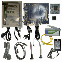
Manufacturer Part Number
MPC8360E-RDK
Description
BOARD REFERENCE DESIGN FOR MPC
Manufacturer
Freescale Semiconductor
Series
PowerQUICC II™ PROr
Type
MPUr
Specifications of MPC8360E-RDK
Contents
Board, Cables, CD, Power Supply
Processor To Be Evaluated
MPC8360E
Data Bus Width
32 bit
Interface Type
RS-232, Ethernet, USB
Operating Supply Voltage
1.3 V
For Use With/related Products
MPC8360E
Lead Free Status / RoHS Status
Lead free / RoHS Compliant


8.2.4.2
Table 34
Figure 19
Freescale Semiconductor
At recommended operating conditions with LV
PMA_RX_CLK clock period
PMA_RX_CLK skew
RX_CLK duty cycle
RCG[9:0] setup time to rising PMA_RX_CLK
RCG[9:0] hold time to rising PMA_RX_CLK
RX_CLK clock rise time, V
RX_CLK clock fall time, V
Notes:
1. The symbols used for timing specifications follow the pattern of t
2. Setup and hold time of even numbered RCG are measured from riding edge of PMA_RX_CLK1. Setup and hold time of odd
inputs and t
timing (TR) with respect to the time data input signals (D) reach the valid state (V) relative to the t
going to the high (H) state or setup time. Also, t
signals (D) went invalid (X) relative to the t
reference symbol representation is based on three letters representing the clock of a particular functional. For example, the
subscript of t
appropriate letter: R (rise) or F (fall). For symbols representing skews, the subscript is skew (SK) followed by the clock that
is being skewed (TRX).
numbered RCG are measured from riding edge of PMA_RX_CLK0.
MPC8360E/MPC8358E PowerQUICC II Pro Processor Revision 2.x TBGA Silicon Hardware Specifications, Rev. 4
provides the TBI receive AC timing specifications.
shows the TBI receive AC timing diagram.
(first two letters of functional block)(reference)(state)(signal)(state)
PMA_RX_CLK1
PMA_RX_CLK0
Parameter/Condition
TRX
TBI Receive AC Timing Specifications
represents the TBI (T) receive (RX) clock. For rise and fall times, the latter convention is used with the
RCG[9:0]
IH
IL
(max) to V
(min) to V
Table 34. TBI Receive AC Timing Specifications
Figure 19. TBI Receive AC Timing Diagram
IH
IL
(min)
(max)
DD
t
SKTRX
t
/OV
TRXH
t
TRDVKH
TRX
DD
clock reference (K) going to the high (H) state. Note that, in general, the clock
TRDXKH
of 3.3 V ± 10%.
t
TRX
t
TRXH
t
symbolizes TBI receive timing (TR) with respect to the time data input
Symbol
TRXH
t
t
TRDVKH
TRDXKH
t
t
Even RCG
SKTRX
t
TRXR
t
TRXF
TRX
/t
TRX
UCC Ethernet Controller: Three-Speed Ethernet, MII Management
1
(first two letters of functional block)(signal)(state)(reference)(state)
for outputs. For example, t
t
TRXF
Min
7.5
2.5
1.0
0.7
0.7
Odd RCG
40
—
t
TRDXKH
t
TRXR
t
TRDVKH
16.0
Typ
—
—
—
—
—
—
t
TRDXKH
TRDVKH
Max
TRX
8.5
2.4
2.4
60
—
—
—
symbolizes TBI receive
clock reference (K)
Unit
ns
ns
ns
ns
ns
ns
%
Notes
for
—
—
—
—
—
2
2
37
Related parts for MPC8360E-RDK
Image
Part Number
Description
Manufacturer
Datasheet
Request
R

Part Number:
Description:
Mpc8360e Powerquicc Ii Pro Family
Manufacturer:
Freescale Semiconductor, Inc
Datasheet:

Part Number:
Description:
BOARD PROCESSOR FOR MPC8360E
Manufacturer:
Freescale Semiconductor
Datasheet:
Part Number:
Description:
Manufacturer:
Freescale Semiconductor, Inc
Datasheet:
Part Number:
Description:
Manufacturer:
Freescale Semiconductor, Inc
Datasheet:
Part Number:
Description:
Manufacturer:
Freescale Semiconductor, Inc
Datasheet:
Part Number:
Description:
Manufacturer:
Freescale Semiconductor, Inc
Datasheet:
Part Number:
Description:
Manufacturer:
Freescale Semiconductor, Inc
Datasheet:
Part Number:
Description:
Manufacturer:
Freescale Semiconductor, Inc
Datasheet:
Part Number:
Description:
Manufacturer:
Freescale Semiconductor, Inc
Datasheet:
Part Number:
Description:
Manufacturer:
Freescale Semiconductor, Inc
Datasheet:
Part Number:
Description:
Manufacturer:
Freescale Semiconductor, Inc
Datasheet:
Part Number:
Description:
Manufacturer:
Freescale Semiconductor, Inc
Datasheet:
Part Number:
Description:
Manufacturer:
Freescale Semiconductor, Inc
Datasheet:
Part Number:
Description:
Manufacturer:
Freescale Semiconductor, Inc
Datasheet:
Part Number:
Description:
Manufacturer:
Freescale Semiconductor, Inc
Datasheet: