MPC8360E-RDK Freescale Semiconductor, MPC8360E-RDK Datasheet - Page 53
MPC8360E-RDK
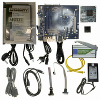
Manufacturer Part Number
MPC8360E-RDK
Description
BOARD REFERENCE DESIGN FOR MPC
Manufacturer
Freescale Semiconductor
Series
PowerQUICC II™ PROr
Type
MPUr
Specifications of MPC8360E-RDK
Contents
Board, Cables, CD, Power Supply
Processor To Be Evaluated
MPC8360E
Data Bus Width
32 bit
Interface Type
RS-232, Ethernet, USB
Operating Supply Voltage
1.3 V
For Use With/related Products
MPC8360E
Lead Free Status / RoHS Status
Lead free / RoHS Compliant


Figure 34
Figure 35
Freescale Semiconductor
All values refer to V
Data hold time:
Rise time of both SDA and SCL signals
Fall time of both SDA and SCL signals
Set-up time for STOP condition
Bus free time between a STOP and START condition
Noise margin at the LOW level for each connected device (including
hysteresis)
Noise margin at the HIGH level for each connected device (including
hysteresis)
Notes:
1. The symbols used for timing specifications follow the pattern of t
2. The device provides a hold time of at least 300 ns for the SDA signal (referred to the V
3. The maximum t
4. C
inputs and t
with respect to the time data input signals (D) reach the valid state (V) relative to the t
(H) state or setup time. Also, t
(S) went invalid (X) relative to the t
timing (I2) for the time that the data with respect to the stop condition (P) reaching the valid state (V) relative to the t
reference (K) going to the high (H) state or setup time. For rise and fall times, the latter convention is used with the appropriate
letter: R (rise) or F (fall).
undefined region of the falling edge of SCL.
MPC8360E/MPC8358E PowerQUICC II Pro Processor Revision 2.x TBGA Silicon Hardware Specifications, Rev. 4
B
SDA
SCL
= capacitance of one bus line in pF.
provides the AC test load for the I
shows the AC timing diagram for the I
(first two letters of functional block)(reference)(state)(signal)(state)
S
IH
I2DVKH
(min) and V
t
I2CF
t
I2CL
t
I2SXKL
has only to be met if the device does not stretch the LOW period (t
Output
Parameter
IL
Table 45. I
(max) levels (see
I2SXKL
I2C
symbolizes I
clock reference (K) going to the low (L) state or hold time. Also, t
Figure 35. I
CBUS compatible masters
t
I2DXKL
2
C AC Electrical Specifications (continued)
Figure 34. I
Table
Z
t
I2DVKH
0
= 50 Ω
2
I
44).
2
t
C timing (I2) for the time that the data with respect to the start condition
2
I2CH
2
C bus devices
C.
C Bus AC Timing Diagram
2
t
I2SXKL
2
C bus.
C AC Test Load
(first two letters of functional block)(signal)(state)(reference)(state)
for outputs. For example, t
Sr
Symbol
t
t
t
I2PVKH
t
I2KHDX
I2DXKL
I2SVKH
t
t
V
V
I2CR
I2CF
t
NH
NL
I2KHKL
R
L
= 50 Ω
1
I2C
20 + 0.1 C
20 + 0.1 C
0.1 × OV
0.2 × OV
IH
t
clock reference (K) going to the high
I2PVKH
min of the SCL signal) to bridge the
Min
OV
0.6
1.3
—
0
I2CL
I2DVKH
2
DD
t
I2CR
) of the SCL signal.
DD
DD
/2
b
b
4
4
symbolizes I
I2PVKH
P
Max
t
0.9
300
300
I2CF
—
—
—
—
—
symbolizes I
3
2
C timing (I2)
S
I2C
Unit
clock
for
μs
ns
ns
μs
μs
V
V
2
C
I
53
2
C
Related parts for MPC8360E-RDK
Image
Part Number
Description
Manufacturer
Datasheet
Request
R

Part Number:
Description:
Mpc8360e Powerquicc Ii Pro Family
Manufacturer:
Freescale Semiconductor, Inc
Datasheet:

Part Number:
Description:
BOARD PROCESSOR FOR MPC8360E
Manufacturer:
Freescale Semiconductor
Datasheet:
Part Number:
Description:
Manufacturer:
Freescale Semiconductor, Inc
Datasheet:
Part Number:
Description:
Manufacturer:
Freescale Semiconductor, Inc
Datasheet:
Part Number:
Description:
Manufacturer:
Freescale Semiconductor, Inc
Datasheet:
Part Number:
Description:
Manufacturer:
Freescale Semiconductor, Inc
Datasheet:
Part Number:
Description:
Manufacturer:
Freescale Semiconductor, Inc
Datasheet:
Part Number:
Description:
Manufacturer:
Freescale Semiconductor, Inc
Datasheet:
Part Number:
Description:
Manufacturer:
Freescale Semiconductor, Inc
Datasheet:
Part Number:
Description:
Manufacturer:
Freescale Semiconductor, Inc
Datasheet:
Part Number:
Description:
Manufacturer:
Freescale Semiconductor, Inc
Datasheet:
Part Number:
Description:
Manufacturer:
Freescale Semiconductor, Inc
Datasheet:
Part Number:
Description:
Manufacturer:
Freescale Semiconductor, Inc
Datasheet:
Part Number:
Description:
Manufacturer:
Freescale Semiconductor, Inc
Datasheet:
Part Number:
Description:
Manufacturer:
Freescale Semiconductor, Inc
Datasheet: