MPC8360E-RDK Freescale Semiconductor, MPC8360E-RDK Datasheet - Page 21
MPC8360E-RDK
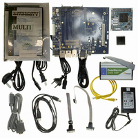
Manufacturer Part Number
MPC8360E-RDK
Description
BOARD REFERENCE DESIGN FOR MPC
Manufacturer
Freescale Semiconductor
Series
PowerQUICC II™ PROr
Type
MPUr
Specifications of MPC8360E-RDK
Contents
Board, Cables, CD, Power Supply
Processor To Be Evaluated
MPC8360E
Data Bus Width
32 bit
Interface Type
RS-232, Ethernet, USB
Operating Supply Voltage
1.3 V
For Use With/related Products
MPC8360E
Lead Free Status / RoHS Status
Lead free / RoHS Compliant


Table 15
Table 16
device when GV
Freescale Semiconductor
Input current (0 V ≤V
Notes:
1. GV
2. MV
3. V
4. Output leakage is measured with all outputs disabled, 0 V
I/O supply voltage
I/O reference voltage
I/O termination voltage
Input high voltage
Input low voltage
Output leakage current
Output high current (V
Output low current (V
MV
Input current (0 V ≤V
Notes:
1. GV
2. MV
3. V
4. Output leakage is measured with all outputs disabled, 0 V
Input/output capacitance: DQ, DQS, DQS
Delta input/output capacitance: DQ, DQS, DQS
Note:
1. This parameter is sampled. GV
on MV
MV
noise on MV
equal to MV
MPC8360E/MPC8358E PowerQUICC II Pro Processor Revision 2.x TBGA Silicon Hardware Specifications, Rev. 4
REF
TT
TT
DD
DD
REF
REF
REF
is not applied directly to the device. It is the supply to which far end signal termination is made and is expected to equal
is not applied directly to the device. It is the supply to which far end signal termination is made and is expected to be
input leakage current
is expected to be within 50 mV of the DRAM GV
is expected to be within 50 mV of the DRAM GV
REF
. This rail should track variations in the DC level of MV
is expected to equal 0.5 × GV
is expected to be equal to 0.5 × GV
provides the DDR2 capacitance when GV
provides the recommended operating conditions for the DDR SDRAM component(s) of the
Table 14. DDR2 SDRAM DC Electrical Characteristics for GV
Parameter/Condition
cannot exceed ±2% of the DC value.
REF
REF
Parameter/Condition
. This rail should track variations in the DC level of MV
Parameter/Condition
Table 16. DDR SDRAM DC Electrical Characteristics for GV
may not exceed ±2% of the DC value.
DD
IN
IN
OUT
OUT
(typ) = 2.5 V.
≤ OV
≤ OV
= 0.35 V)
= 1.95 V)
DD
DD
Table 15. DDR2 SDRAM Capacitance for GV
)
)
DD
= 1.8 V ± 0.090 V, f = 1 MHz, T
DD
, and to track GV
DD
, and to track GV
Symbol
I
IN
Symbol
DD
DD
MV
GV
I
VREF
DD
V
I
V
I
V
I
I
OZ
OH
OL
at all times.
IN
at all times.
TT
≤
≤
REF
IH
IL
DD
DD
DC variations as measured at the receiver. Peak-to-peak noise
V
V
REF
Symbol
(typ) = 1.8 V.
OUT
OUT
DD
C
C
.
DIO
A
IO
DC variations as measured at the receiver. Peak-to-peak
Min
≤
≤
—
= 25°C, V
MV
MV
GV
GV
0.49 × GV
REF
REF
REF
DD
DD
2.375
–15.2
–0.3
15.2
Min
.
—
—
—
.
.
– 0.04
+ 0.18
OUT
Min
DD
DD
—
6
DD
(typ)=1.8 V
= GV
(typ) = 1.8 V (continued)
MV
MV
DD
0.51 × GV
DD
GV
Max
±10
/2, V
REF
REF
(typ) = 2.5 V
2.625
DD
Max
±10
±10
±10
—
—
Max
0.5
+ 0.04
+ 0.3
– 0.18
OUT
8
DD
(peak-to-peak) = 0.2 V.
DDR and DDR2 SDRAM
Unit
Unit
Unit
μA
mA
mA
pF
pF
μA
μA
μA
V
V
V
V
V
Notes
Notes
Notes
—
—
—
—
—
—
—
1
1
2
4
1
3
21
Related parts for MPC8360E-RDK
Image
Part Number
Description
Manufacturer
Datasheet
Request
R

Part Number:
Description:
Mpc8360e Powerquicc Ii Pro Family
Manufacturer:
Freescale Semiconductor, Inc
Datasheet:

Part Number:
Description:
BOARD PROCESSOR FOR MPC8360E
Manufacturer:
Freescale Semiconductor
Datasheet:
Part Number:
Description:
Manufacturer:
Freescale Semiconductor, Inc
Datasheet:
Part Number:
Description:
Manufacturer:
Freescale Semiconductor, Inc
Datasheet:
Part Number:
Description:
Manufacturer:
Freescale Semiconductor, Inc
Datasheet:
Part Number:
Description:
Manufacturer:
Freescale Semiconductor, Inc
Datasheet:
Part Number:
Description:
Manufacturer:
Freescale Semiconductor, Inc
Datasheet:
Part Number:
Description:
Manufacturer:
Freescale Semiconductor, Inc
Datasheet:
Part Number:
Description:
Manufacturer:
Freescale Semiconductor, Inc
Datasheet:
Part Number:
Description:
Manufacturer:
Freescale Semiconductor, Inc
Datasheet:
Part Number:
Description:
Manufacturer:
Freescale Semiconductor, Inc
Datasheet:
Part Number:
Description:
Manufacturer:
Freescale Semiconductor, Inc
Datasheet:
Part Number:
Description:
Manufacturer:
Freescale Semiconductor, Inc
Datasheet:
Part Number:
Description:
Manufacturer:
Freescale Semiconductor, Inc
Datasheet:
Part Number:
Description:
Manufacturer:
Freescale Semiconductor, Inc
Datasheet: