DK-DEV-3CLS200N Altera, DK-DEV-3CLS200N Datasheet - Page 11
DK-DEV-3CLS200N
Manufacturer Part Number
DK-DEV-3CLS200N
Description
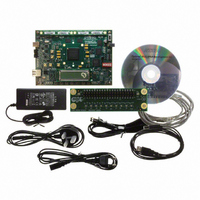
KIT DEV CYCLONE III LS EP3CLS200
Manufacturer
Altera
Series
Cyclone® IIIr
Type
FPGAr
Datasheets
1.EP3C5F256C8N.pdf
(34 pages)
2.EP3C5F256C8N.pdf
(14 pages)
3.DK-START-3C25N.pdf
(74 pages)
4.DK-DEV-3CLS200N.pdf
(42 pages)
Specifications of DK-DEV-3CLS200N
Contents
Board
Silicon Manufacturer
Altera
Core Architecture
FPGA
Core Sub-architecture
Cyclone
Silicon Core Number
EP3C
Silicon Family Name
Cyclone III LS
Rohs Compliant
Yes
For Use With/related Products
EP3CLS200
Lead Free Status / RoHS Status
Lead free / RoHS Compliant
Other names
544-2601


Chapter 1: Cyclone III Device Data Sheet
Electrical Characteristics
Table 1–12. Hysteresis Specifications for Schmitt Trigger Input in Cyclone III Devices
Table 1–13. Cyclone III Devices Single-Ended I/O Standard Specifications
© January 2010 Altera Corporation
V
3.3-V LVTTL
3.3-V LVCMOS
3.0-V LVTTL
3.0-V LVCMOS
2.5-V LVTTL and
LVCMOS
1.8-V LVTTL and
LVCMOS
1.5-V LVCMOS
1.2-V LVCMOS
3.0-V PCI
3.0-V PCI-X
Notes to
(1) For voltage referenced receiver input waveform and explanation of terms used in
(2) AC load CL = 10 pF.
(3) For more detail about interfacing Cyclone III devices with 3.3/3.0/2.5-V LVTTL/LVCMOS I/O standards, refer to
S CHM ITT
I/O Standard
Symbol
in
Devices with 3.3/3.0/2.5-V LVTTL and LVCMOS I/O
“Glossary” on page
Table
(3)
(3)
(3)
1–13:
(3)
(3)
Hysteresis for Schmitt trigger
input
3.135
3.135
2.375
1.425
2.85
2.85
1.71
1.14
2.85
2.85
Min
I/O Standard Specifications
The following tables list input voltage sensitivities (V
and V
supported by Cyclone III devices.
standard specifications for Cyclone III devices.
1–27.
Parameter
V
OL
CC IO
Typ
3.3
3.3
3.0
3.0
2.5
1.8
1.5
1.2
3.0
3.0
), and current drive characteristics (I
(V)
3.465
3.465
2.625
1.575
3.15
Max
3.15
3.15
1.89
1.26
3.15
–0.3
–0.3
–0.3
–0.3
–0.3
–0.3
Min
Systems.
—
—
—
—
V
V
V
V
V
IL
Conditions
CC IO
CC IO
CC IO
CC IO
(V)
0.35 *
0.35 *
0.35 *
0.35*
0.3 *
Max
V
V
V
V
V
0.8
0.8
0.8
0.8
0.7
CCIO
= 3.3 V
= 2.5 V
= 1.8 V
= 1.5 V
CCIO
CCIO
CCIO
CCIO
Table 1–13
0.65 *
0.65 *
0.65 *
0.5 *
0.5 *
Min
V
V
V
V
V
1.7
1.7
1.7
1.7
1.7
CC IO
CC IO
CC IO
CC IO
CC IO
Minimum
V
Table
IH
200
200
140
110
V
V
V
V
V
V
V
(V)
C CIO
C CIO
C CIO
C CIO
C CIO
C CIO
C CIO
OH
Max
2.25
1–13, refer to
through
(Note
3.6
3.6
+ 0.3
+ 0.3
+ 0.3
+ 0.3
+ 0.3
+ 0.3
+ 0.3
and I
1),
OL
0.25 * V
0.25 * V
IH
(2)
) for various I/O standards
0.1 * V
0.1 * V
Table 1–18
Typical
“Single-ended Voltage referenced I/O Standard”
V
and V
Max
0.45
0.45
0.45
—
—
—
—
0.2
0.2
0.4
OL
Cyclone III Device Handbook, Volume 2
(V)
CC IO
CC IO
C CIO
C CIO
IL
), output voltage (V
AN 447: Interfacing Cyclone III
V
0.75 * V
0.75 * V
provide the I/O
V
V
0.9 * V
0.9 * V
CC IO
C CIO
C CIO
V
Maximum
Min
O H
2.4
2.4
2.0
– 0.45
– 0.2
– 0.2
(V)
—
—
—
—
C CIO
C CIO
CC IO
CC IO
(mA)
0.1
1.5
1.5
I
4
2
4
1
2
2
2
O L
Unit
mV
mV
mV
mV
1–11
OH
(mA)
–0.1
–0.5
–0.5
–4
–2
–4
–1
–2
–2
–2
I
O H
Related parts for DK-DEV-3CLS200N
Image
Part Number
Description
Manufacturer
Datasheet
Request
R

Part Number:
Description:
KIT DEV ARRIA II GX FPGA 2AGX125
Manufacturer:
Altera
Datasheet:

Part Number:
Description:
KIT DEV STRATIX IV FPGA 4SE530
Manufacturer:
Altera
Datasheet:

Part Number:
Description:
KIT DEV FPGA 2AGX260 W/6.375G TX
Manufacturer:
Altera
Datasheet:

Part Number:
Description:
KIT DEV MAX V 5M570Z
Manufacturer:
Altera
Datasheet:

Part Number:
Description:
KIT DEV STRATIX V FPGA 5SGXEA7
Manufacturer:
Altera
Datasheet:

Part Number:
Description:
KIT DEVELOPMENT STRATIX III
Manufacturer:
Altera
Datasheet:

Part Number:
Description:
KIT DEVELOPMENT STRATIX IV
Manufacturer:
Altera
Datasheet:

Part Number:
Description:
KIT DEV ARRIA GX 1AGX60N
Manufacturer:
Altera
Datasheet:
Part Number:
Description:
KIT STARTER CYCLONE IV GX
Manufacturer:
Altera
Datasheet:
Part Number:
Description:
KIT DEVELOPMENT STRATIX IV
Manufacturer:
Altera
Datasheet:

Part Number:
Description:
CPLD, EP610 Family, ECMOS Process, 300 Gates, 16 Macro Cells, 16 Reg., 16 User I/Os, 5V Supply, 35 Speed Grade, 24DIP
Manufacturer:
Altera Corporation
Datasheet:
Part Number:
Description:
CPLD, EP610 Family, ECMOS Process, 300 Gates, 16 Macro Cells, 16 Reg., 16 User I/Os, 5V Supply, 15 Speed Grade, 24DIP
Manufacturer:
Altera Corporation
Datasheet: