DK-DEV-3CLS200N Altera, DK-DEV-3CLS200N Datasheet - Page 30
DK-DEV-3CLS200N
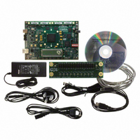
Manufacturer Part Number
DK-DEV-3CLS200N
Description
KIT DEV CYCLONE III LS EP3CLS200
Manufacturer
Altera
Series
Cyclone® IIIr
Type
FPGAr
Datasheets
1.EP3C5F256C8N.pdf
(34 pages)
2.EP3C5F256C8N.pdf
(14 pages)
3.DK-START-3C25N.pdf
(74 pages)
4.DK-DEV-3CLS200N.pdf
(42 pages)
Specifications of DK-DEV-3CLS200N
Contents
Board
Silicon Manufacturer
Altera
Core Architecture
FPGA
Core Sub-architecture
Cyclone
Silicon Core Number
EP3C
Silicon Family Name
Cyclone III LS
Rohs Compliant
Yes
For Use With/related Products
EP3CLS200
Lead Free Status / RoHS Status
Lead free / RoHS Compliant
Other names
544-2601


1–30
Table 1–39. Glossary (Part 4 of 5)
Cyclone III Device Handbook, Volume 2
Letter
U
T
t
TCCS (Channel-
to-channel-skew)
tcin
t
tcout
t
t
t
Timing Unit
Interval (TUI)
t
t
t
tpllcin
tpllcout
Transmitter
Output Waveform
t
t
C
C O
DUTY
FA LL
H
INJITTER
OUTJITTER_DEDC LK
OUTJITTER_IO
RISE
S U
Term
—
High-speed receiver/transmitter input and output clock period.
HIGH-SPEED I/O Block: The timing difference between the fastest and slowest output edges,
including t
Delay from clock pad to I/O input register.
Delay from clock pad to I/O output.
Delay from clock pad to I/O output register.
HIGH-SPEED I/O Block: Duty cycle on high-speed transmitter output clock.
Signal High-to-low transition time (80–20%).
Input register hold time.
HIGH-SPEED I/O block: The timing budget allowed for skew, propagation delays, and data
sampling window. (TUI = 1/(Receiver Input Clock Frequency Multiplication Factor) = t
Period jitter on PLL clock input.
Period jitter on dedicated clock output driven by a PLL.
Period jitter on general purpose I/O driven by a PLL.
Delay from PLL inclk pad to I/O input register.
Delay from PLL inclk pad to I/O output register.
Transmitter Output Waveforms for the LVDS, mini-LVDS, PPDS and RSDS Differential I/O
Standards
Signal Low-to-high transition time (20–80%).
Input register setup time.
Single-Ended Waveform
Differential Waveform (Mathematical Function of Positive & Negative Channel)
C O
variation and clock skew. The clock is included in the TCCS measurement.
V os
V
OD
V
OD
Definitions
—
Chapter 1: Cyclone III Device Data Sheet
V
OD
© January 2010 Altera Corporation
Positive Channel (p) = V
Negative Channel (n) = V
Ground
0 V
p - n
C
/w).
OH
OL
Glossary
Related parts for DK-DEV-3CLS200N
Image
Part Number
Description
Manufacturer
Datasheet
Request
R

Part Number:
Description:
KIT DEV ARRIA II GX FPGA 2AGX125
Manufacturer:
Altera
Datasheet:

Part Number:
Description:
KIT DEV STRATIX IV FPGA 4SE530
Manufacturer:
Altera
Datasheet:

Part Number:
Description:
KIT DEV FPGA 2AGX260 W/6.375G TX
Manufacturer:
Altera
Datasheet:

Part Number:
Description:
KIT DEV MAX V 5M570Z
Manufacturer:
Altera
Datasheet:

Part Number:
Description:
KIT DEV STRATIX V FPGA 5SGXEA7
Manufacturer:
Altera
Datasheet:

Part Number:
Description:
KIT DEVELOPMENT STRATIX III
Manufacturer:
Altera
Datasheet:

Part Number:
Description:
KIT DEVELOPMENT STRATIX IV
Manufacturer:
Altera
Datasheet:

Part Number:
Description:
KIT DEV ARRIA GX 1AGX60N
Manufacturer:
Altera
Datasheet:
Part Number:
Description:
KIT STARTER CYCLONE IV GX
Manufacturer:
Altera
Datasheet:
Part Number:
Description:
KIT DEVELOPMENT STRATIX IV
Manufacturer:
Altera
Datasheet:

Part Number:
Description:
CPLD, EP610 Family, ECMOS Process, 300 Gates, 16 Macro Cells, 16 Reg., 16 User I/Os, 5V Supply, 35 Speed Grade, 24DIP
Manufacturer:
Altera Corporation
Datasheet:
Part Number:
Description:
CPLD, EP610 Family, ECMOS Process, 300 Gates, 16 Macro Cells, 16 Reg., 16 User I/Os, 5V Supply, 15 Speed Grade, 24DIP
Manufacturer:
Altera Corporation
Datasheet: