DK-DEV-3CLS200N Altera, DK-DEV-3CLS200N Datasheet - Page 29
DK-DEV-3CLS200N
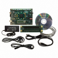
Manufacturer Part Number
DK-DEV-3CLS200N
Description
KIT DEV CYCLONE III LS EP3CLS200
Manufacturer
Altera
Series
Cyclone® IIIr
Type
FPGAr
Datasheets
1.EP3C5F256C8N.pdf
(34 pages)
2.EP3C5F256C8N.pdf
(14 pages)
3.DK-START-3C25N.pdf
(74 pages)
4.DK-DEV-3CLS200N.pdf
(42 pages)
Specifications of DK-DEV-3CLS200N
Contents
Board
Silicon Manufacturer
Altera
Core Architecture
FPGA
Core Sub-architecture
Cyclone
Silicon Core Number
EP3C
Silicon Family Name
Cyclone III LS
Rohs Compliant
Yes
For Use With/related Products
EP3CLS200
Lead Free Status / RoHS Status
Lead free / RoHS Compliant
Other names
544-2601


Chapter 1: Cyclone III Device Data Sheet
Glossary
Table 1–39. Glossary (Part 3 of 5)
© January 2010 Altera Corporation
Letter
R
S
R
Receiver Input
Waveform
RSKM (Receiver
input skew
margin)
Single-ended
Voltage
referenced I/O
Standard
SW (Sampling
Window)
L
Term
Receiver differential input discrete resistor (external to Cyclone III devices).
Receiver Input Waveform for LVDS and LVPECL Differential Standards.
HIGH-SPEED I/O Block: The total margin left after accounting for the sampling window and TCCS.
RSKM = (TUI – SW – TCCS) / 2.
The JEDEC standard for SSTl and HSTL I/O standards defines both the AC and DC input signal
values. The AC values indicate the voltage levels at which the receiver must meet its timing
specifications. The DC values indicate the voltage levels at which the final logic state of the
receiver is unambiguously defined. After the receiver input crosses the AC value, the receiver
changes to the new logic state. The new logic state is then maintained as long as the input stays
beyond the DC threshold. This approach is intended to provide predictable receiver timing in the
presence of input waveform ringing.
HIGH-SPEED I/O Block: The period of time during which the data must be valid to capture it
correctly. The setup and hold times determine the ideal strobe position in the sampling window.
Single-Ended Waveform
Differential Waveform (Mathematical Function of Positive & Negative Channel)
V
V
OH
OL
V
CM
V
ID
V
ID
Definitions
V
REF
Cyclone III Device Handbook, Volume 2
V
ID
Positive Channel (p) = V
Negative Channel (n) = V
Ground
0 V
p - n
V
V
IH(DC)
IL(DC)
V
V
IH ( AC )
IL(AC )
V
CCIO
V
IH
IL
SS
1–29
Related parts for DK-DEV-3CLS200N
Image
Part Number
Description
Manufacturer
Datasheet
Request
R

Part Number:
Description:
KIT DEV ARRIA II GX FPGA 2AGX125
Manufacturer:
Altera
Datasheet:

Part Number:
Description:
KIT DEV STRATIX IV FPGA 4SE530
Manufacturer:
Altera
Datasheet:

Part Number:
Description:
KIT DEV FPGA 2AGX260 W/6.375G TX
Manufacturer:
Altera
Datasheet:

Part Number:
Description:
KIT DEV MAX V 5M570Z
Manufacturer:
Altera
Datasheet:

Part Number:
Description:
KIT DEV STRATIX V FPGA 5SGXEA7
Manufacturer:
Altera
Datasheet:

Part Number:
Description:
KIT DEVELOPMENT STRATIX III
Manufacturer:
Altera
Datasheet:

Part Number:
Description:
KIT DEVELOPMENT STRATIX IV
Manufacturer:
Altera
Datasheet:

Part Number:
Description:
KIT DEV ARRIA GX 1AGX60N
Manufacturer:
Altera
Datasheet:
Part Number:
Description:
KIT STARTER CYCLONE IV GX
Manufacturer:
Altera
Datasheet:
Part Number:
Description:
KIT DEVELOPMENT STRATIX IV
Manufacturer:
Altera
Datasheet:

Part Number:
Description:
CPLD, EP610 Family, ECMOS Process, 300 Gates, 16 Macro Cells, 16 Reg., 16 User I/Os, 5V Supply, 35 Speed Grade, 24DIP
Manufacturer:
Altera Corporation
Datasheet:
Part Number:
Description:
CPLD, EP610 Family, ECMOS Process, 300 Gates, 16 Macro Cells, 16 Reg., 16 User I/Os, 5V Supply, 15 Speed Grade, 24DIP
Manufacturer:
Altera Corporation
Datasheet: