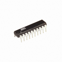
ATTINY2313-20PU Atmel, ATTINY2313-20PU Datasheet - Page 123

ATTINY2313-20PU
Manufacturer Part Number
ATTINY2313-20PU
Description
IC MCU AVR 2K FLASH 20DIP
Manufacturer
Atmel
Series
AVR® ATtinyr
Datasheets
1.ATTINY2313-20MU.pdf
(226 pages)
2.ATTINY2313V-10MU.pdf
(15 pages)
3.ATTINY2313V-10SU.pdf
(20 pages)
Specifications of ATTINY2313-20PU
Core Processor
AVR
Core Size
8-Bit
Speed
20MHz
Connectivity
SPI, UART/USART
Peripherals
Brown-out Detect/Reset, POR, PWM, WDT
Number Of I /o
18
Program Memory Size
2KB (1K x 16)
Program Memory Type
FLASH
Eeprom Size
128 x 8
Ram Size
128 x 8
Voltage - Supply (vcc/vdd)
2.7 V ~ 5.5 V
Oscillator Type
Internal
Operating Temperature
-40°C ~ 85°C
Package / Case
20-DIP (0.300", 7.62mm)
Package
20PDIP
Device Core
AVR
Family Name
ATtiny
Maximum Speed
20 MHz
Operating Supply Voltage
3.3|5 V
Data Bus Width
8 Bit
Number Of Programmable I/os
18
Interface Type
SPI/USART/USI
Number Of Timers
2
Processor Series
ATTINY2x
Core
AVR8
Data Ram Size
128 B
Maximum Clock Frequency
20 MHz
Maximum Operating Temperature
+ 85 C
Mounting Style
Through Hole
3rd Party Development Tools
EWAVR, EWAVR-BL
Development Tools By Supplier
ATAVRDRAGON, ATSTK500, ATSTK600, ATAVRISP2, ATAVRONEKIT
Minimum Operating Temperature
- 40 C
Cpu Family
ATtiny
Device Core Size
8b
Frequency (max)
20MHz
Total Internal Ram Size
128Byte
# I/os (max)
18
Number Of Timers - General Purpose
2
Operating Supply Voltage (typ)
3.3/5V
Operating Supply Voltage (max)
5.5V
Operating Supply Voltage (min)
2.7V
Instruction Set Architecture
RISC
Operating Temp Range
-40C to 85C
Operating Temperature Classification
Industrial
Mounting
Through Hole
Pin Count
20
Package Type
PDIP
For Use With
ATSTK600-DIP40 - STK600 SOCKET/ADAPTER 40-PDIP770-1007 - ISP 4PORT ATMEL AVR MCU SPI/JTAGATAVRDRAGON - KIT DRAGON 32KB FLASH MEM AVRATAVRISP2 - PROGRAMMER AVR IN SYSTEMATJTAGICE2 - AVR ON-CHIP D-BUG SYSTEM
Lead Free Status / RoHS Status
Lead free / RoHS Compliant
Data Converters
-
Lead Free Status / Rohs Status
Lead free / RoHS Compliant
Available stocks
Company
Part Number
Manufacturer
Quantity
Price
Part Number:
ATTINY2313-20PU
Manufacturer:
ATMEL/爱特梅尔
Quantity:
20 000
Receive Compete Flag
and Interrupt
Receiver Error Flags
2543L–AVR–08/10
Note:
The receive function example reads all the I/O Registers into the Register File before any com-
putation is done. This gives an optimal receive buffer utilization since the buffer location read will
be free to accept new data as early as possible.
The USART Receiver has one flag that indicates the Receiver state.
The Receive Complete (RXC) flag indicates if there are unread data present in the receive buf-
fer. This flag is one when unread data exist in the receive buffer, and zero when the receive
buffer is empty (i.e., does not contain any unread data). If the Receiver is disabled (RXEN = 0),
the receive buffer will be flushed and consequently the RXC bit will become zero.
When the Receive Complete Interrupt Enable (RXCIE) in UCSRB is set, the USART Receive
Complete interrupt will be executed as long as the RXC flag is set (provided that global inter-
rupts are enabled). When interrupt-driven data reception is used, the receive complete routine
must read the received data from UDR in order to clear the RXC flag, otherwise a new interrupt
will occur once the interrupt routine terminates.
The USART Receiver has three error flags: Frame Error (FE), Data OverRun (DOR) and Parity
Error (UPE). All can be accessed by reading UCSRA. Common for the error flags is that they are
located in the receive buffer together with the frame for which they indicate the error status. Due
to the buffering of the error flags, the UCSRA must be read before the receive buffer (UDR),
since reading the UDR I/O location changes the buffer read location. Another equality for the
error flags is that they can not be altered by software doing a write to the flag location. However,
all flags must be set to zero when the UCSRA is written for upward compatibility of future
USART implementations. None of the error flags can generate interrupts.
The Frame Error (FE) flag indicates the state of the first stop bit of the next readable frame
stored in the receive buffer. The FE flag is zero when the stop bit was correctly read (as one),
and the FE flag will be one when the stop bit was incorrect (zero). This flag can be used for
detecting out-of-sync conditions, detecting break conditions and protocol handling. The FE flag
is not affected by the setting of the USBS bit in UCSRC since the Receiver ignores all, except for
the first, stop bits. For compatibility with future devices, always set this bit to zero when writing to
UCSRA.
The Data OverRun (DOR) flag indicates data loss due to a receiver buffer full condition. A Data
OverRun occurs when the receive buffer is full (two characters), it is a new character waiting in
the Receive Shift Register, and a new start bit is detected. If the DOR flag is set there was one
or more serial frame lost between the frame last read from UDR, and the next frame read from
UDR. For compatibility with future devices, always write this bit to zero when writing to UCSRA.
The DOR flag is cleared when the frame received was successfully moved from the Shift Regis-
ter to the receive buffer.
The Parity Error (UPE) Flag indicates that the next frame in the receive buffer had a Parity Error
when received. If Parity Check is not enabled the UPE bit will always be read zero. For compati-
bility with future devices, always set this bit to zero when writing to UCSRA. For more details see
“Parity Bit Calculation” on page 115
1. The example code assumes that the part specific header file is included.
For I/O Registers located in extended I/O map, “IN”, “OUT”, “SBIS”, “SBIC”, “CBI”, and “SBI”
instructions must be replaced with instructions that allow access to extended I/O. Typically
“LDS” and “STS” combined with “SBRS”, “SBRC”, “SBR”, and “CBR”.
and
“Parity Checker” on page
124.
123


