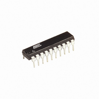
ATTINY2313-20PU Atmel, ATTINY2313-20PU Datasheet - Page 129

ATTINY2313-20PU
Manufacturer Part Number
ATTINY2313-20PU
Description
IC MCU AVR 2K FLASH 20DIP
Manufacturer
Atmel
Series
AVR® ATtinyr
Datasheets
1.ATTINY2313-20MU.pdf
(226 pages)
2.ATTINY2313V-10MU.pdf
(15 pages)
3.ATTINY2313V-10SU.pdf
(20 pages)
Specifications of ATTINY2313-20PU
Core Processor
AVR
Core Size
8-Bit
Speed
20MHz
Connectivity
SPI, UART/USART
Peripherals
Brown-out Detect/Reset, POR, PWM, WDT
Number Of I /o
18
Program Memory Size
2KB (1K x 16)
Program Memory Type
FLASH
Eeprom Size
128 x 8
Ram Size
128 x 8
Voltage - Supply (vcc/vdd)
2.7 V ~ 5.5 V
Oscillator Type
Internal
Operating Temperature
-40°C ~ 85°C
Package / Case
20-DIP (0.300", 7.62mm)
Package
20PDIP
Device Core
AVR
Family Name
ATtiny
Maximum Speed
20 MHz
Operating Supply Voltage
3.3|5 V
Data Bus Width
8 Bit
Number Of Programmable I/os
18
Interface Type
SPI/USART/USI
Number Of Timers
2
Processor Series
ATTINY2x
Core
AVR8
Data Ram Size
128 B
Maximum Clock Frequency
20 MHz
Maximum Operating Temperature
+ 85 C
Mounting Style
Through Hole
3rd Party Development Tools
EWAVR, EWAVR-BL
Development Tools By Supplier
ATAVRDRAGON, ATSTK500, ATSTK600, ATAVRISP2, ATAVRONEKIT
Minimum Operating Temperature
- 40 C
Cpu Family
ATtiny
Device Core Size
8b
Frequency (max)
20MHz
Total Internal Ram Size
128Byte
# I/os (max)
18
Number Of Timers - General Purpose
2
Operating Supply Voltage (typ)
3.3/5V
Operating Supply Voltage (max)
5.5V
Operating Supply Voltage (min)
2.7V
Instruction Set Architecture
RISC
Operating Temp Range
-40C to 85C
Operating Temperature Classification
Industrial
Mounting
Through Hole
Pin Count
20
Package Type
PDIP
For Use With
ATSTK600-DIP40 - STK600 SOCKET/ADAPTER 40-PDIP770-1007 - ISP 4PORT ATMEL AVR MCU SPI/JTAGATAVRDRAGON - KIT DRAGON 32KB FLASH MEM AVRATAVRISP2 - PROGRAMMER AVR IN SYSTEMATJTAGICE2 - AVR ON-CHIP D-BUG SYSTEM
Lead Free Status / RoHS Status
Lead free / RoHS Compliant
Data Converters
-
Lead Free Status / Rohs Status
Lead free / RoHS Compliant
Available stocks
Company
Part Number
Manufacturer
Quantity
Price
Part Number:
ATTINY2313-20PU
Manufacturer:
ATMEL/爱特梅尔
Quantity:
20 000
USART Register
Description
USART I/O Data
Register – UDR
USART Control and
Status Register A –
UCSRA
2543L–AVR–08/10
The USART Transmit Data Buffer Register and USART Receive Data Buffer Registers share the
same I/O address referred to as USART Data Register or UDR. The Transmit Data Buffer Reg-
ister (TXB) will be the destination for data written to the UDR Register location. Reading the
UDR Register location will return the contents of the Receive Data Buffer Register (RXB).
For 5-, 6-, or 7-bit characters the upper unused bits will be ignored by the Transmitter and set to
zero by the Receiver.
The transmit buffer can only be written when the UDRE flag in the UCSRA Register is set. Data
written to UDR when the UDRE flag is not set, will be ignored by the USART Transmitter. When
data is written to the transmit buffer, and the Transmitter is enabled, the Transmitter will load the
data into the Transmit Shift Register when the Shift Register is empty. Then the data will be seri-
ally transmitted on the TxD pin.
The receive buffer consists of a two level FIFO. The FIFO will change its state whenever the
receive buffer is accessed. Due to this behavior of the receive buffer, do not use Read-Modify-
Write instructions (SBI and CBI) on this location. Be careful when using bit test instructions
(SBIC and SBIS), since these also will change the state of the FIFO.
• Bit 7 – RXC: USART Receive Complete
This flag bit is set when there are unread data in the receive buffer and cleared when the receive
buffer is empty (i.e., does not contain any unread data). If the Receiver is disabled, the receive
buffer will be flushed and consequently the RXC bit will become zero. The RXC flag can be used
to generate a Receive Complete interrupt (see description of the RXCIE bit).
• Bit 6 – TXC: USART Transmit Complete
This flag bit is set when the entire frame in the Transmit Shift Register has been shifted out and
there are no new data currently present in the transmit buffer (UDR). The TXC flag bit is auto-
matically cleared when a transmit complete interrupt is executed, or it can be cleared by writing
a one to its bit location. The TXC flag can generate a Transmit Complete interrupt (see descrip-
tion of the TXCIE bit).
Bit
Read/Write
Initial Value
Bit
Read/Write
Initial Value
R/W
RXC
7
0
R
7
0
R/W
TXC
R/W
6
0
6
0
UDRE
R/W
5
0
R
5
1
R/W
4
0
FE
4
R
0
RXB[7:0]
TXB[7:0]
R/W
DOR
3
0
R
3
0
R/W
UPE
2
0
R
2
0
R/W
1
0
U2X
R/W
1
0
R/W
MPCM
0
0
R/W
0
0
UDR (Read)
UDR (Write)
UCSRA
129


