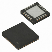
ATTINY25V-10MU Atmel, ATTINY25V-10MU Datasheet - Page 116

ATTINY25V-10MU
Manufacturer Part Number
ATTINY25V-10MU
Description
IC MCU AVR 2K FLASH 10MHZ 20-QFN
Manufacturer
Atmel
Series
AVR® ATtinyr
Specifications of ATTINY25V-10MU
Core Processor
AVR
Core Size
8-Bit
Speed
10MHz
Connectivity
USI
Peripherals
Brown-out Detect/Reset, POR, PWM, WDT
Number Of I /o
6
Program Memory Size
2KB (1K x 16)
Program Memory Type
FLASH
Eeprom Size
128 x 8
Ram Size
128 x 8
Voltage - Supply (vcc/vdd)
1.8 V ~ 5.5 V
Data Converters
A/D 4x10b
Oscillator Type
Internal
Operating Temperature
-40°C ~ 85°C
Package / Case
20-MLF®, QFN
Processor Series
ATTINY2x
Core
AVR8
Data Bus Width
8 bit
Data Ram Size
128 B
Interface Type
USI
Maximum Clock Frequency
10 MHz
Number Of Programmable I/os
6
Number Of Timers
2
Operating Supply Voltage
1.8 V to 5.5 V
Maximum Operating Temperature
+ 85 C
Mounting Style
SMD/SMT
Minimum Operating Temperature
- 40 C
On-chip Adc
4-ch x 10-bit
For Use With
ATSTK600-DIP40 - STK600 SOCKET/ADAPTER 40-PDIPATAVRBC100 - REF DESIGN KIT BATTERY CHARGER770-1007 - ISP 4PORT ATMEL AVR MCU SPI/JTAGATAVRDRAGON - KIT DRAGON 32KB FLASH MEM AVRATAVRISP2 - PROGRAMMER AVR IN SYSTEMATJTAGICE2 - AVR ON-CHIP D-BUG SYSTEM
Lead Free Status / RoHS Status
Lead free / RoHS Compliant
Available stocks
Company
Part Number
Manufacturer
Quantity
Price
Company:
Part Number:
ATTINY25V-10MU
Manufacturer:
ATMEL
Quantity:
1 650
Part Number:
ATTINY25V-10MU
Manufacturer:
ATMEL/爱特梅尔
Quantity:
20 000
116
ATtiny25/45/85
Figure 15-4
is only the physical layer that is shown since the system operation is highly dependent of the
communication scheme used. The main differences between the master and slave operation at
this level is the serial clock generation which is always done by the master. Only the slave uses
the clock control unit.
Clock generation must be implemented in software, but the shift operation is done automatically
in both devices. Note that clocking only on negative edges for shifting data is of practical use in
this mode. The slave can insert wait states at start or end of transfer by forcing the SCL clock
low. This means that the master must always check if the SCL line was actually released after it
has generated a positive edge.
Since the clock also increments the counter, a counter overflow can be used to indicate that the
transfer is completed. The clock is generated by the master by toggling the USCK pin via the
PORTB register.
The data direction is not given by the physical layer. A protocol, like the one used by the TWI-
bus, must be implemented to control the data flow.
Figure 15-5. Two-wire Mode, Typical Timing Diagram
Referring to the timing diagram
SDA
SCL
1. The start condition is generated by the master by forcing the SDA low line while keep-
2. In addition, the start detector will hold the SCL line low after the master has forced a
3. The master set the first bit to be transferred and releases the SCL line (C). The slave
4. After eight bits containing slave address and data direction (read or write) have been
5. When the slave is addressed, it holds the SDA line low during the acknowledgment
ing the SCL line high (A). SDA can be forced low either by writing a zero to bit 7 of the
USI Data Register, or by setting the corresponding bit in the PORTB register to zero.
Note that the Data Direction Register bit must be set to one for the output to be
enabled. The start detector logic of the slave device (see
detects the start condition and sets the USISIF Flag. The flag can generate an interrupt
if necessary.
negative edge on this line (B). This allows the slave to wake up from sleep or complete
other tasks before setting up the USI Data Register to receive the address. This is done
by clearing the start condition flag and resetting the counter.
samples the data and shifts it into the USI Data Register at the positive edge of the SCL
clock.
transferred, the slave counter overflows and the SCL line is forced low (D). If the slave
is not the one the master has addressed, it releases the SCL line and waits for a new
start condition.
cycle before holding the SCL line low again (i.e., the USI Counter Register must be set
to 14 before releasing SCL at (D)). Depending on the R/W bit the master or slave
shows two USI units operating in two-wire mode, one as master and one as slave. It
S
A B
C
ADDRESS
1 - 7
R/W
(Figure
8
D
15-5), a bus transfer involves the following steps:
ACK
9
E
DATA
1 - 8
ACK
9
Figure 15-6 on page
DATA
1 - 8
ACK
9
2586M–AVR–07/10
117)
P
F


