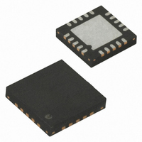
ATTINY25V-10MU Atmel, ATTINY25V-10MU Datasheet - Page 38

ATTINY25V-10MU
Manufacturer Part Number
ATTINY25V-10MU
Description
IC MCU AVR 2K FLASH 10MHZ 20-QFN
Manufacturer
Atmel
Series
AVR® ATtinyr
Specifications of ATTINY25V-10MU
Core Processor
AVR
Core Size
8-Bit
Speed
10MHz
Connectivity
USI
Peripherals
Brown-out Detect/Reset, POR, PWM, WDT
Number Of I /o
6
Program Memory Size
2KB (1K x 16)
Program Memory Type
FLASH
Eeprom Size
128 x 8
Ram Size
128 x 8
Voltage - Supply (vcc/vdd)
1.8 V ~ 5.5 V
Data Converters
A/D 4x10b
Oscillator Type
Internal
Operating Temperature
-40°C ~ 85°C
Package / Case
20-MLF®, QFN
Processor Series
ATTINY2x
Core
AVR8
Data Bus Width
8 bit
Data Ram Size
128 B
Interface Type
USI
Maximum Clock Frequency
10 MHz
Number Of Programmable I/os
6
Number Of Timers
2
Operating Supply Voltage
1.8 V to 5.5 V
Maximum Operating Temperature
+ 85 C
Mounting Style
SMD/SMT
Minimum Operating Temperature
- 40 C
On-chip Adc
4-ch x 10-bit
For Use With
ATSTK600-DIP40 - STK600 SOCKET/ADAPTER 40-PDIPATAVRBC100 - REF DESIGN KIT BATTERY CHARGER770-1007 - ISP 4PORT ATMEL AVR MCU SPI/JTAGATAVRDRAGON - KIT DRAGON 32KB FLASH MEM AVRATAVRISP2 - PROGRAMMER AVR IN SYSTEMATJTAGICE2 - AVR ON-CHIP D-BUG SYSTEM
Lead Free Status / RoHS Status
Lead free / RoHS Compliant
Available stocks
Company
Part Number
Manufacturer
Quantity
Price
Company:
Part Number:
ATTINY25V-10MU
Manufacturer:
ATMEL
Quantity:
1 650
Part Number:
ATTINY25V-10MU
Manufacturer:
ATMEL/爱特梅尔
Quantity:
20 000
7.4.3
7.4.4
7.4.5
7.4.6
7.5
7.5.1
38
Register Description
ATtiny25/45/85
Brown-out Detector
Internal Voltage Reference
Watchdog Timer
Port Pins
MCUCR – MCU Control Register
If the Brown-out Detector is not needed in the application, this module should be turned off. If the
Brown-out Detector is enabled by the BODLEVEL Fuses, it will be enabled in all sleep modes,
and hence, always consume power. In the deeper sleep modes, this will contribute significantly
to the total current consumption. See
able” on page 36
The Internal Voltage Reference will be enabled when needed by the Brown-out Detection, the
Analog Comparator or the ADC. If these modules are disabled as described in the sections
above, the internal voltage reference will be disabled and it will not be consuming power. When
turned on again, the user must allow the reference to start up before the output is used. If the
reference is kept on in sleep mode, the output can be used immediately. Refer to
age Reference” on page 44
If the Watchdog Timer is not needed in the application, this module should be turned off. If the
Watchdog Timer is enabled, it will be enabled in all sleep modes, and hence, always consume
power. In the deeper sleep modes, this will contribute significantly to the total current consump-
tion. Refer to
When entering a sleep mode, all port pins should be configured to use minimum power. The
most important thing is then to ensure that no pins drive resistive loads. In sleep modes where
both the I/O clock (clk
will be disabled. This ensures that no power is consumed by the input logic when not needed. In
some cases, the input logic is needed for detecting wake-up conditions, and it will then be
enabled. Refer to the section
which pins are enabled. If the input buffer is enabled and the input signal is left floating or has an
analog signal level close to V
For analog input pins, the digital input buffer should be disabled at all times. An analog signal
level close to V
input buffers can be disabled by writing to the Digital Input Disable Register (DIDR0). Refer to
“DIDR0 – Digital Input Disable Register 0” on page 125
The MCU Control Register contains control bits for power management.
• Bit 7 – BODS: BOD Sleep
BOD disable functionality is available in some devices, only. See
In order to disable BOD during sleep (see
logic one. This is controlled by a timed sequence and the enable bit, BODSE in MCUCR. First,
Bit
0x35
Read/Write
Initial Value
“Watchdog Timer” on page 44
CC
BODS
R
7
0
for details on how to configure the Brown-out Detector.
/2 on an input pin can cause significant current even in active mode. Digital
I/O
) and the ADC clock (clk
PUD
R/W
6
0
for details on the start-up time.
CC
“Digital Input Enable and Sleep Modes” on page 59
/2, the input buffer will use excessive power.
R/W
SE
5
0
“Brown-out Detection” on page 43
Table 7-1 on page
SM1
R/W
for details on how to configure the Watchdog Timer.
4
0
ADC
) are stopped, the input buffers of the device
SM0
R/W
3
0
for details.
BODSE
35) the BODS bit must be written to
R
2
0
“Limitations” on page
ISC01
R/W
1
0
and
“Software BOD Dis-
ISC00
R/W
0
0
2586M–AVR–07/10
“Internal Volt-
for details on
37.
MCUCR


