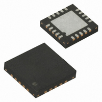
ATTINY25V-10MU Atmel, ATTINY25V-10MU Datasheet - Page 118

ATTINY25V-10MU
Manufacturer Part Number
ATTINY25V-10MU
Description
IC MCU AVR 2K FLASH 10MHZ 20-QFN
Manufacturer
Atmel
Series
AVR® ATtinyr
Specifications of ATTINY25V-10MU
Core Processor
AVR
Core Size
8-Bit
Speed
10MHz
Connectivity
USI
Peripherals
Brown-out Detect/Reset, POR, PWM, WDT
Number Of I /o
6
Program Memory Size
2KB (1K x 16)
Program Memory Type
FLASH
Eeprom Size
128 x 8
Ram Size
128 x 8
Voltage - Supply (vcc/vdd)
1.8 V ~ 5.5 V
Data Converters
A/D 4x10b
Oscillator Type
Internal
Operating Temperature
-40°C ~ 85°C
Package / Case
20-MLF®, QFN
Processor Series
ATTINY2x
Core
AVR8
Data Bus Width
8 bit
Data Ram Size
128 B
Interface Type
USI
Maximum Clock Frequency
10 MHz
Number Of Programmable I/os
6
Number Of Timers
2
Operating Supply Voltage
1.8 V to 5.5 V
Maximum Operating Temperature
+ 85 C
Mounting Style
SMD/SMT
Minimum Operating Temperature
- 40 C
On-chip Adc
4-ch x 10-bit
For Use With
ATSTK600-DIP40 - STK600 SOCKET/ADAPTER 40-PDIPATAVRBC100 - REF DESIGN KIT BATTERY CHARGER770-1007 - ISP 4PORT ATMEL AVR MCU SPI/JTAGATAVRDRAGON - KIT DRAGON 32KB FLASH MEM AVRATAVRISP2 - PROGRAMMER AVR IN SYSTEMATJTAGICE2 - AVR ON-CHIP D-BUG SYSTEM
Lead Free Status / RoHS Status
Lead free / RoHS Compliant
Available stocks
Company
Part Number
Manufacturer
Quantity
Price
Company:
Part Number:
ATTINY25V-10MU
Manufacturer:
ATMEL
Quantity:
1 650
Part Number:
ATTINY25V-10MU
Manufacturer:
ATMEL/爱特梅尔
Quantity:
20 000
- Current page: 118 of 236
- Download datasheet (5Mb)
15.4.4
15.4.5
15.5
15.5.1
15.5.2
118
Register Descriptions
ATtiny25/45/85
Edge Triggered External Interrupt
Software Interrupt
USIDR – USI Data Register
USIBR – USI Buffer Register
By setting the counter to maximum value (F) it can function as an additional external interrupt.
The Overflow Flag and Interrupt Enable bit are then used for the external interrupt. This feature
is selected by the USICS1 bit.
The counter overflow interrupt can be used as a software interrupt triggered by a clock strobe.
The USI Data Register can be accessed directly but a copy of the data can also be found in the
USI Buffer Register.
Depending on the USICS[1:0] bits of the USI Control Register a (left) shift operation may be per-
formed. The shift operation can be synchronised to an external clock edge, to a Timer/Counter0
Compare Match, or directly to software via the USICLK bit. If a serial clock occurs at the same
cycle the register is written, the register will contain the value written and no shift is performed.
Note that even when no wire mode is selected (USIWM[1:0] = 0) both the external data input
(DI/SDA) and the external clock input (USCK/SCL) can still be used by the USI Data Register.
The output pin (DO or SDA, depending on the wire mode) is connected via the output latch to
the most significant bit (bit 7) of the USI Data Register. The output latch ensures that data input
is sampled and data output is changed on opposite clock edges. The latch is open (transparent)
during the first half of a serial clock cycle when an external clock source is selected (USICS1 =
1) and constantly open when an internal clock source is used (USICS1 = 0). The output will be
changed immediately when a new MSB is written as long as the latch is open.
Note that the Data Direction Register bit corresponding to the output pin must be set to one in
order to enable data output from the USI Data Register.
Instead of reading data from the USI Data Register the USI Buffer Register can be used. This
makes controlling the USI less time critical and gives the CPU more time to handle other pro-
gram tasks. USI flags as set similarly as when reading the USIDR register.
The content of the USI Data Register is loaded to the USI Buffer Register when the transfer has
been completed.
Bit
0x0F
Read/Write
Initial Value
Bit
0x10
Read/Write
Initial Value
MSB
MSB
R/W
R
7
0
7
0
R/W
R
6
0
6
0
R/W
R
5
0
5
0
R/W
R
4
0
4
0
R/W
R
3
0
3
0
R/W
R
2
0
2
0
R/W
R
1
0
1
0
LSB
R/W
LSB
0
0
0
R
0
2586M–AVR–07/10
USIDR
USIBR
Related parts for ATTINY25V-10MU
Image
Part Number
Description
Manufacturer
Datasheet
Request
R

Part Number:
Description:
MCU AVR 2K FLASH 4MHZ 8-SOIC
Manufacturer:
Atmel
Datasheet:

Part Number:
Description:
MCU AVR 2KB FLASH 10MHZ 8SOIC
Manufacturer:
Atmel
Datasheet:

Part Number:
Description:
IC AVR MCU 2K 10MHZ 8-DIP
Manufacturer:
Atmel
Datasheet:

Part Number:
Description:
IC MCU AVR 2KB FLASH 10MHZ 8SOIC
Manufacturer:
Atmel
Datasheet:

Part Number:
Description:
IC MCU AVR 2KB FLASH 10MHZ 8SOIC
Manufacturer:
Atmel
Datasheet:

Part Number:
Description:
MCU AVR 2KB FLASH 10MHZ 8SOIC
Manufacturer:
Atmel
Datasheet:

Part Number:
Description:
MCU AVR 2KB FLASH 10MHZ 20QFN
Manufacturer:
Atmel
Datasheet:

Part Number:
Description:
MCU AVR 2K ISP FLASH 1.8V 8-SOIC
Manufacturer:
Atmel
Datasheet:

Part Number:
Description:
IC AVR MCU 2K 10MHZ 8DIP
Manufacturer:
Atmel
Datasheet:

Part Number:
Description:
IC AVR MCU 2K 10MHZ 8SOIC
Manufacturer:
Atmel
Datasheet:

Part Number:
Description:
8-bit Microcontrollers - MCU 2KB FLASH,128B EE, 128B SRAM-10MHz
Manufacturer:
Atmel

Part Number:
Description:
8-bit Microcontrollers - MCU 2KB FL,128B EE,128B SRAM-10MHz
Manufacturer:
Atmel

Part Number:
Description:
8-bit Microcontrollers - MCU AVR 16KB FL 512B EE 1KB SRAM 10 MHZ GRN
Manufacturer:
Atmel


