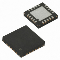
ATTINY25V-10MU Atmel, ATTINY25V-10MU Datasheet - Page 88

ATTINY25V-10MU
Manufacturer Part Number
ATTINY25V-10MU
Description
IC MCU AVR 2K FLASH 10MHZ 20-QFN
Manufacturer
Atmel
Series
AVR® ATtinyr
Specifications of ATTINY25V-10MU
Core Processor
AVR
Core Size
8-Bit
Speed
10MHz
Connectivity
USI
Peripherals
Brown-out Detect/Reset, POR, PWM, WDT
Number Of I /o
6
Program Memory Size
2KB (1K x 16)
Program Memory Type
FLASH
Eeprom Size
128 x 8
Ram Size
128 x 8
Voltage - Supply (vcc/vdd)
1.8 V ~ 5.5 V
Data Converters
A/D 4x10b
Oscillator Type
Internal
Operating Temperature
-40°C ~ 85°C
Package / Case
20-MLF®, QFN
Processor Series
ATTINY2x
Core
AVR8
Data Bus Width
8 bit
Data Ram Size
128 B
Interface Type
USI
Maximum Clock Frequency
10 MHz
Number Of Programmable I/os
6
Number Of Timers
2
Operating Supply Voltage
1.8 V to 5.5 V
Maximum Operating Temperature
+ 85 C
Mounting Style
SMD/SMT
Minimum Operating Temperature
- 40 C
On-chip Adc
4-ch x 10-bit
For Use With
ATSTK600-DIP40 - STK600 SOCKET/ADAPTER 40-PDIPATAVRBC100 - REF DESIGN KIT BATTERY CHARGER770-1007 - ISP 4PORT ATMEL AVR MCU SPI/JTAGATAVRDRAGON - KIT DRAGON 32KB FLASH MEM AVRATAVRISP2 - PROGRAMMER AVR IN SYSTEMATJTAGICE2 - AVR ON-CHIP D-BUG SYSTEM
Lead Free Status / RoHS Status
Lead free / RoHS Compliant
Available stocks
Company
Part Number
Manufacturer
Quantity
Price
Company:
Part Number:
ATTINY25V-10MU
Manufacturer:
ATMEL
Quantity:
1 650
Part Number:
ATTINY25V-10MU
Manufacturer:
ATMEL/爱特梅尔
Quantity:
20 000
- Current page: 88 of 236
- Download datasheet (5Mb)
88
ATtiny25/45/85
Figure 12-3. Timer/Counter1 Block Diagram
Three status flags (overflow and compare matches) are found in the Timer/Counter Interrupt
Flag Register - TIFR. Control signals are found in the Timer/Counter Control Registers TCCR1
and GTCCR. The interrupt enable/disable settings are found in the Timer/Counter Interrupt
Mask Register - TIMSK.
The Timer/Counter1 contains three Output Compare Registers, OCR1A, OCR1B, and OCR1C
as the data source to be compared with the Timer/Counter1 contents. In normal mode the Out-
put Compare functions are operational with all three output compare registers. OCR1A
determines action on the OC1A pin (PB1), and it can generate Timer1 OC1A interrupt in normal
mode and in PWM mode. Likewise, OCR1B determines action on the OC1B pin (PB4) and it can
generate Timer1 OC1B interrupt in normal mode and in PWM mode. OCR1C holds the
Timer/Counter maximum value, i.e. the clear on compare match value. In the normal mode an
overflow interrupt (TOV1) is generated when Timer/Counter1 counts from $FF to $00, while in
the PWM mode the overflow interrupt is generated when Timer/Counter1 counts either from $FF
to $00 or from OCR1C to $00. The inverted PWM outputs OC1A and OC1B are not connected in
normal mode.
In PWM mode, OCR1A and OCR1B provide the data values against which the Timer Counter
value is compared. Upon compare match the PWM outputs (OC1A, OC1A, OC1B, OC1B) are
generated. In PWM mode, the Timer Counter counts up to the value specified in the output com-
pare register OCR1C and starts again from $00. This feature allows limiting the counter “full”
value to a specified value, lower than $FF. Together with the many prescaler options, flexible
PWM frequency selection is provided.
8-BIT DATABUS
COMPARE REGISTER
TIMER/COUNTER1
8-BIT COMPARATOR
REGISTER (TIMSK)
TIMER/COUNTER1
TIMER INT. MASK
T/C1 OUTPUT
T/C1 OVER-
FLOW IRQ
(OCR1A)
(TCNT1)
T/C1 COMPARE
MATCH A IRQ
T/C CLEAR
REGISTER (TIFR)
TIMER INT. FLAG
T/C1 COMPARE
MATCH B IRQ
COMPARE REGISTER
8-BIT COMPARATOR
T/C1 OUTPUT
(OCR1B)
Table 12-3 on page 91
DEAD TIME GENERATOR
OC1A
(PB1)
REGISTER 1 (TCCR1)
T/C1 CONTROL
T/C CONTROL
LOGIC
OC1A
(PB0)
lists clock selection and OCR1C
COMPARE REGISTER
OC1B
(PB4)
DEAD TIME GENERATOR
8-BIT COMPARATOR
T/C1 OUTPUT
(OCR1C)
GLOBAL T/C CONTROL
REGISTER (GTCCR)
OC1B
(PB3)
2586M–AVR–07/10
CK
PCK
Related parts for ATTINY25V-10MU
Image
Part Number
Description
Manufacturer
Datasheet
Request
R

Part Number:
Description:
MCU AVR 2K FLASH 4MHZ 8-SOIC
Manufacturer:
Atmel
Datasheet:

Part Number:
Description:
MCU AVR 2KB FLASH 10MHZ 8SOIC
Manufacturer:
Atmel
Datasheet:

Part Number:
Description:
IC AVR MCU 2K 10MHZ 8-DIP
Manufacturer:
Atmel
Datasheet:

Part Number:
Description:
IC MCU AVR 2KB FLASH 10MHZ 8SOIC
Manufacturer:
Atmel
Datasheet:

Part Number:
Description:
IC MCU AVR 2KB FLASH 10MHZ 8SOIC
Manufacturer:
Atmel
Datasheet:

Part Number:
Description:
MCU AVR 2KB FLASH 10MHZ 8SOIC
Manufacturer:
Atmel
Datasheet:

Part Number:
Description:
MCU AVR 2KB FLASH 10MHZ 20QFN
Manufacturer:
Atmel
Datasheet:

Part Number:
Description:
MCU AVR 2K ISP FLASH 1.8V 8-SOIC
Manufacturer:
Atmel
Datasheet:

Part Number:
Description:
IC AVR MCU 2K 10MHZ 8DIP
Manufacturer:
Atmel
Datasheet:

Part Number:
Description:
IC AVR MCU 2K 10MHZ 8SOIC
Manufacturer:
Atmel
Datasheet:

Part Number:
Description:
8-bit Microcontrollers - MCU 2KB FLASH,128B EE, 128B SRAM-10MHz
Manufacturer:
Atmel

Part Number:
Description:
8-bit Microcontrollers - MCU 2KB FL,128B EE,128B SRAM-10MHz
Manufacturer:
Atmel

Part Number:
Description:
8-bit Microcontrollers - MCU AVR 16KB FL 512B EE 1KB SRAM 10 MHZ GRN
Manufacturer:
Atmel


