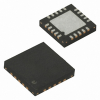
ATTINY25V-10MU Atmel, ATTINY25V-10MU Datasheet - Page 151

ATTINY25V-10MU
Manufacturer Part Number
ATTINY25V-10MU
Description
IC MCU AVR 2K FLASH 10MHZ 20-QFN
Manufacturer
Atmel
Series
AVR® ATtinyr
Specifications of ATTINY25V-10MU
Core Processor
AVR
Core Size
8-Bit
Speed
10MHz
Connectivity
USI
Peripherals
Brown-out Detect/Reset, POR, PWM, WDT
Number Of I /o
6
Program Memory Size
2KB (1K x 16)
Program Memory Type
FLASH
Eeprom Size
128 x 8
Ram Size
128 x 8
Voltage - Supply (vcc/vdd)
1.8 V ~ 5.5 V
Data Converters
A/D 4x10b
Oscillator Type
Internal
Operating Temperature
-40°C ~ 85°C
Package / Case
20-MLF®, QFN
Processor Series
ATTINY2x
Core
AVR8
Data Bus Width
8 bit
Data Ram Size
128 B
Interface Type
USI
Maximum Clock Frequency
10 MHz
Number Of Programmable I/os
6
Number Of Timers
2
Operating Supply Voltage
1.8 V to 5.5 V
Maximum Operating Temperature
+ 85 C
Mounting Style
SMD/SMT
Minimum Operating Temperature
- 40 C
On-chip Adc
4-ch x 10-bit
For Use With
ATSTK600-DIP40 - STK600 SOCKET/ADAPTER 40-PDIPATAVRBC100 - REF DESIGN KIT BATTERY CHARGER770-1007 - ISP 4PORT ATMEL AVR MCU SPI/JTAGATAVRDRAGON - KIT DRAGON 32KB FLASH MEM AVRATAVRISP2 - PROGRAMMER AVR IN SYSTEMATJTAGICE2 - AVR ON-CHIP D-BUG SYSTEM
Lead Free Status / RoHS Status
Lead free / RoHS Compliant
Available stocks
Company
Part Number
Manufacturer
Quantity
Price
Company:
Part Number:
ATTINY25V-10MU
Manufacturer:
ATMEL
Quantity:
1 650
Part Number:
ATTINY25V-10MU
Manufacturer:
ATMEL/爱特梅尔
Quantity:
20 000
- Current page: 151 of 236
- Download datasheet (5Mb)
20. Memory Programming
20.1
2586M–AVR–07/10
Program And Data Memory Lock Bits
This section describes the different methods for Programming the ATtiny25/45/85 memories.
ATtiny25/45/85 provides two Lock bits which can be left unprogrammed (“1”) or can be pro-
grammed (“0”) to obtain the additional security listed in
“1” with the Chip Erase command, only.
Program memory can be read out via the debugWIRE interface when the DWEN fuse is pro-
grammed, even if the Lock Bits are set. Thus, when Lock Bit security is required debugWIRE
should always be disabled (by clearing the DWEN fuse).
Table 20-1.
Note:
Table 20-2.
Notes:
Lock bits can also be read by device firmware. See section
Data from Software” on page
LB Mode
1
2
3
Lock Bit
1. “1” means unprogrammed, “0” means programmed
1. Program the Fuse bits before programming the LB1 and LB2.
2. “1” means unprogrammed, “0” means programmed
Memory Lock Bits
LB2
LB1
Lock Bit Byte
Lock Bit Protection Modes
LB2
1
1
0
(1)
LB1
147.
1
0
0
Bit No
7
6
5
4
3
2
1
0
Protection Type
No memory lock features enabled.
Further programming of the Flash and EEPROM is disabled in
High-voltage and Serial Programming mode. The Fuse bits are
locked in both Serial and High-voltage Programming mode.
debugWire is disabled.
Further programming and verification of the Flash and EEPROM
is disabled in High-voltage and Serial Programming mode. The
Fuse bits are locked in both Serial and High-voltage
Programming mode.
(1)(2)
Description
–
–
–
–
–
–
Lock bit
Lock bit
(1)
Table
debugWire is disabled.
“Reading Lock, Fuse and Signature
20-2. Lock bits can be erased to
Default Value
1 (unprogrammed)
1 (unprogrammed)
1 (unprogrammed)
1 (unprogrammed)
1 (unprogrammed)
1 (unprogrammed)
1 (unprogrammed)
1 (unprogrammed)
(1)
151
Related parts for ATTINY25V-10MU
Image
Part Number
Description
Manufacturer
Datasheet
Request
R

Part Number:
Description:
MCU AVR 2K FLASH 4MHZ 8-SOIC
Manufacturer:
Atmel
Datasheet:

Part Number:
Description:
MCU AVR 2KB FLASH 10MHZ 8SOIC
Manufacturer:
Atmel
Datasheet:

Part Number:
Description:
IC AVR MCU 2K 10MHZ 8-DIP
Manufacturer:
Atmel
Datasheet:

Part Number:
Description:
IC MCU AVR 2KB FLASH 10MHZ 8SOIC
Manufacturer:
Atmel
Datasheet:

Part Number:
Description:
IC MCU AVR 2KB FLASH 10MHZ 8SOIC
Manufacturer:
Atmel
Datasheet:

Part Number:
Description:
MCU AVR 2KB FLASH 10MHZ 8SOIC
Manufacturer:
Atmel
Datasheet:

Part Number:
Description:
MCU AVR 2KB FLASH 10MHZ 20QFN
Manufacturer:
Atmel
Datasheet:

Part Number:
Description:
MCU AVR 2K ISP FLASH 1.8V 8-SOIC
Manufacturer:
Atmel
Datasheet:

Part Number:
Description:
IC AVR MCU 2K 10MHZ 8DIP
Manufacturer:
Atmel
Datasheet:

Part Number:
Description:
IC AVR MCU 2K 10MHZ 8SOIC
Manufacturer:
Atmel
Datasheet:

Part Number:
Description:
8-bit Microcontrollers - MCU 2KB FLASH,128B EE, 128B SRAM-10MHz
Manufacturer:
Atmel

Part Number:
Description:
8-bit Microcontrollers - MCU 2KB FL,128B EE,128B SRAM-10MHz
Manufacturer:
Atmel

Part Number:
Description:
8-bit Microcontrollers - MCU AVR 16KB FL 512B EE 1KB SRAM 10 MHZ GRN
Manufacturer:
Atmel


