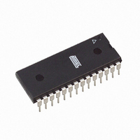
ATMEGA8A-PU Atmel, ATMEGA8A-PU Datasheet - Page 226

ATMEGA8A-PU
Manufacturer Part Number
ATMEGA8A-PU
Description
MCU AVR 8K FLASH 16MHZ 28-PDIP
Manufacturer
Atmel
Series
AVR® ATmegar
Specifications of ATMEGA8A-PU
Core Processor
AVR
Core Size
8-Bit
Speed
16MHz
Connectivity
I²C, SPI, UART/USART
Peripherals
Brown-out Detect/Reset, POR, PWM, WDT
Number Of I /o
23
Program Memory Size
8KB (4K x 16)
Program Memory Type
FLASH
Eeprom Size
512 x 8
Ram Size
1K x 8
Voltage - Supply (vcc/vdd)
2.7 V ~ 5.5 V
Data Converters
A/D 6x10b
Oscillator Type
Internal
Operating Temperature
-40°C ~ 85°C
Package / Case
28-DIP (0.300", 7.62mm)
Processor Series
ATMEGA8x
Core
AVR8
Data Bus Width
8 bit
Data Ram Size
1 KB
Interface Type
SPI, TWI, USART
Maximum Clock Frequency
16 MHz
Number Of Programmable I/os
23
Number Of Timers
3
Maximum Operating Temperature
+ 85 C
Mounting Style
Through Hole
3rd Party Development Tools
EWAVR, EWAVR-BL
Development Tools By Supplier
ATAVRDRAGON, ATSTK500, ATSTK600, ATAVRISP2, ATAVRONEKIT
Minimum Operating Temperature
- 40 C
On-chip Adc
10 bit, 6 Channel
Package
28PDIP
Device Core
AVR
Family Name
ATmega
Maximum Speed
16 MHz
Operating Supply Voltage
3.3|5 V
Controller Family/series
AVR MEGA
No. Of I/o's
23
Eeprom Memory Size
512Byte
Ram Memory Size
1KB
Cpu Speed
16MHz
Rohs Compliant
Yes
For Use With
ATSTK600 - DEV KIT FOR AVR/AVR32ATSTK500 - PROGRAMMER AVR STARTER KIT
Lead Free Status / RoHS Status
Lead free / RoHS Compliant
Available stocks
Company
Part Number
Manufacturer
Quantity
Price
Part Number:
ATMEGA8A-PU
Manufacturer:
ATMEL/爱特梅尔
Quantity:
20 000
- Current page: 226 of 308
- Download datasheet (6Mb)
24. Memory Programming
24.1
8159D–AVR–02/11
Program And Data Memory Lock Bits
The ATmega8A provides six Lock Bits which can be left unprogrammed (“1”) or can be pro-
grammed (“0”) to obtain the additional features listed in
erased to “1” with the Chip Erase command.
Table 24-1.
Note:
Table 24-2.
BLB12
BLB11
BLB02
BLB01
LB2
LB1
BLB0 Mode
LB Mode
Lock Bit Byte
1
2
3
1
2
3
4
1. “1” means unprogrammed, “0” means programmed
Memory Lock Bits
Lock Bit Byte
Lock Bit Protection Modes
BLB02
LB2
1
1
0
1
1
0
0
BLB01
LB1
Bit No.
1
0
0
1
0
0
1
7
6
5
4
3
2
1
0
Protection Type
No memory lock features enabled.
Further programming of the Flash and EEPROM is disabled in
Parallel and Serial Programming mode. The Fuse Bits are
locked in both Serial and Parallel Programming mode.
Further programming and verification of the Flash and
EEPROM is disabled in parallel and Serial Programming mode.
The Fuse Bits are locked in both Serial and Parallel
Programming modes.
No restrictions for SPM or LPM accessing the Application
section.
SPM is not allowed to write to the Application section.
SPM is not allowed to write to the Application section, and LPM
executing from the Boot Loader section is not allowed to read
from the Application section. If Interrupt Vectors are placed in
the Boot Loader section, interrupts are disabled while executing
from the Application section.
LPM executing from the Boot Loader section is not allowed to
read from the Application section. If Interrupt Vectors are placed
in the Boot Loader section, interrupts are disabled while
executing from the Application section.
(2)
Description
–
–
Boot lock bit
Boot lock bit
Boot lock bit
Boot lock bit
Lock bit
Lock bit
(1)
Table
24-2. The Lock Bits can only be
Default Value
1 (unprogrammed)
1 (unprogrammed)
1 (unprogrammed)
1 (unprogrammed)
1 (unprogrammed)
1 (unprogrammed)
1 (unprogrammed)
1 (unprogrammed)
ATmega8A
(1)
(1)
226
Related parts for ATMEGA8A-PU
Image
Part Number
Description
Manufacturer
Datasheet
Request
R

Part Number:
Description:
IC AVR MCU 8K 16MHZ 5V 32TQFP
Manufacturer:
Atmel
Datasheet:

Part Number:
Description:
IC AVR MCU 8K 16MHZ 5V 32-QFN
Manufacturer:
Atmel
Datasheet:

Part Number:
Description:
IC AVR MCU 8K 16MHZ 5V 28DIP
Manufacturer:
Atmel
Datasheet:

Part Number:
Description:
IC AVR MCU 8K 16MHZ COM 32-TQFP
Manufacturer:
Atmel
Datasheet:

Part Number:
Description:
IC AVR MCU 8K 16MHZ IND 32-TQFP
Manufacturer:
Atmel
Datasheet:

Part Number:
Description:
IC AVR MCU 8K 16MHZ COM 28-DIP
Manufacturer:
Atmel
Datasheet:

Part Number:
Description:
IC AVR MCU 8K 16MHZ IND 28-DIP
Manufacturer:
Atmel
Datasheet:

Part Number:
Description:
IC AVR MCU 8K 16MHZ COM 32-QFN
Manufacturer:
Atmel
Datasheet:

Part Number:
Description:
MCU AVR 8KB FLASH 16MHZ 32QFN
Manufacturer:
Atmel
Datasheet:

Part Number:
Description:
IC AVR MCU 8K 16MHZ IND 32-QFN
Manufacturer:
Atmel
Datasheet:

Part Number:
Description:
IC MCU AVR 8K 5V 16MHZ 32-TQFP
Manufacturer:
Atmel
Datasheet:

Part Number:
Description:
IC MCU AVR 8K 5V 16MHZ 32-QFN
Manufacturer:
Atmel
Datasheet:

Part Number:
Description:
IC MCU AVR 8K 5V 16MHZ 28-DIP
Manufacturer:
Atmel
Datasheet:


