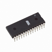
ATMEGA8A-PU Atmel, ATMEGA8A-PU Datasheet - Page 87

ATMEGA8A-PU
Manufacturer Part Number
ATMEGA8A-PU
Description
MCU AVR 8K FLASH 16MHZ 28-PDIP
Manufacturer
Atmel
Series
AVR® ATmegar
Specifications of ATMEGA8A-PU
Core Processor
AVR
Core Size
8-Bit
Speed
16MHz
Connectivity
I²C, SPI, UART/USART
Peripherals
Brown-out Detect/Reset, POR, PWM, WDT
Number Of I /o
23
Program Memory Size
8KB (4K x 16)
Program Memory Type
FLASH
Eeprom Size
512 x 8
Ram Size
1K x 8
Voltage - Supply (vcc/vdd)
2.7 V ~ 5.5 V
Data Converters
A/D 6x10b
Oscillator Type
Internal
Operating Temperature
-40°C ~ 85°C
Package / Case
28-DIP (0.300", 7.62mm)
Processor Series
ATMEGA8x
Core
AVR8
Data Bus Width
8 bit
Data Ram Size
1 KB
Interface Type
SPI, TWI, USART
Maximum Clock Frequency
16 MHz
Number Of Programmable I/os
23
Number Of Timers
3
Maximum Operating Temperature
+ 85 C
Mounting Style
Through Hole
3rd Party Development Tools
EWAVR, EWAVR-BL
Development Tools By Supplier
ATAVRDRAGON, ATSTK500, ATSTK600, ATAVRISP2, ATAVRONEKIT
Minimum Operating Temperature
- 40 C
On-chip Adc
10 bit, 6 Channel
Package
28PDIP
Device Core
AVR
Family Name
ATmega
Maximum Speed
16 MHz
Operating Supply Voltage
3.3|5 V
Controller Family/series
AVR MEGA
No. Of I/o's
23
Eeprom Memory Size
512Byte
Ram Memory Size
1KB
Cpu Speed
16MHz
Rohs Compliant
Yes
For Use With
ATSTK600 - DEV KIT FOR AVR/AVR32ATSTK500 - PROGRAMMER AVR STARTER KIT
Lead Free Status / RoHS Status
Lead free / RoHS Compliant
Available stocks
Company
Part Number
Manufacturer
Quantity
Price
Part Number:
ATMEGA8A-PU
Manufacturer:
ATMEL/爱特梅尔
Quantity:
20 000
- Current page: 87 of 308
- Download datasheet (6Mb)
16.7
8159D–AVR–02/11
Output Compare Units
Register has been read. After a change of the edge, the Input Capture Flag (ICF1) must be
cleared by software (writing a logical one to the I/O bit location). For measuring frequency only,
the clearing of the ICF1 Flag is not required (if an interrupt handler is used).
The 16-bit comparator continuously compares TCNT1 with the Output Compare Register
(OCR1x). If TCNT equals OCR1x the comparator signals a match. A match will set the Output
Compare Flag (OCF1x) at the next timer clock cycle. If enabled (OCIE1x = 1), the Output Com-
pare Flag generates an Output Compare interrupt. The OCF1x Flag is automatically cleared
when the interrupt is executed. Alternatively the OCF1x Flag can be cleared by software by writ-
ing a logical one to its I/O bit location. The waveform generator uses the match signal to
generate an output according to operating mode set by the Waveform Generation mode
(WGM13:0) bits and Compare Output mode (COM1x1:0) bits. The TOP and BOTTOM signals
are used by the waveform generator for handling the special cases of the extreme values in
some modes of operation
A special feature of Output Compare unit A allows it to define the Timer/Counter TOP value (i.e.
counter resolution). In addition to the counter resolution, the TOP value defines the period time
for waveforms generated by the waveform generator.
Figure 16-4
bit names indicates the device number (n = 1 for Timer/Counter 1), and the “x” indicates Output
Compare unit (A/B). The elements of the block diagram that are not directly a part of the Output
Compare unit are gray shaded.
Figure 16-4. Output Compare Unit, Block Diagram
shows a block diagram of the Output Compare unit. The small “n” in the register and
OCRnxH Buf. (8-bit)
OCRnxH (8-bit)
BOTTOM
OCRnx Buffer (16-bit Register)
(See “Modes of Operation” on page
TEMP (8-bit)
TOP
OCRnx (16-bit Register)
OCRnxL Buf. (8-bit)
OCRnxL (8-bit)
DATA BUS
Waveform Generator
=
WGMn3:0
(16-bit Comparator )
(8-bit)
COMnx1:0
TCNTnH (8-bit)
OCFnx (Int.Req.)
90.)
TCNTn (16-bit Counter)
ATmega8A
TCNTnL (8-bit)
OCnx
87
Related parts for ATMEGA8A-PU
Image
Part Number
Description
Manufacturer
Datasheet
Request
R

Part Number:
Description:
IC AVR MCU 8K 16MHZ 5V 32TQFP
Manufacturer:
Atmel
Datasheet:

Part Number:
Description:
IC AVR MCU 8K 16MHZ 5V 32-QFN
Manufacturer:
Atmel
Datasheet:

Part Number:
Description:
IC AVR MCU 8K 16MHZ 5V 28DIP
Manufacturer:
Atmel
Datasheet:

Part Number:
Description:
IC AVR MCU 8K 16MHZ COM 32-TQFP
Manufacturer:
Atmel
Datasheet:

Part Number:
Description:
IC AVR MCU 8K 16MHZ IND 32-TQFP
Manufacturer:
Atmel
Datasheet:

Part Number:
Description:
IC AVR MCU 8K 16MHZ COM 28-DIP
Manufacturer:
Atmel
Datasheet:

Part Number:
Description:
IC AVR MCU 8K 16MHZ IND 28-DIP
Manufacturer:
Atmel
Datasheet:

Part Number:
Description:
IC AVR MCU 8K 16MHZ COM 32-QFN
Manufacturer:
Atmel
Datasheet:

Part Number:
Description:
MCU AVR 8KB FLASH 16MHZ 32QFN
Manufacturer:
Atmel
Datasheet:

Part Number:
Description:
IC AVR MCU 8K 16MHZ IND 32-QFN
Manufacturer:
Atmel
Datasheet:

Part Number:
Description:
IC MCU AVR 8K 5V 16MHZ 32-TQFP
Manufacturer:
Atmel
Datasheet:

Part Number:
Description:
IC MCU AVR 8K 5V 16MHZ 32-QFN
Manufacturer:
Atmel
Datasheet:

Part Number:
Description:
IC MCU AVR 8K 5V 16MHZ 28-DIP
Manufacturer:
Atmel
Datasheet:


