HD6417727BP100BV Renesas Electronics America, HD6417727BP100BV Datasheet - Page 46
HD6417727BP100BV
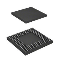
Manufacturer Part Number
HD6417727BP100BV
Description
IC SUPERH MPU ROMLESS 240BGA
Manufacturer
Renesas Electronics America
Series
SuperH® SH7700r
Datasheet
1.HD6417727BP100CV.pdf
(1098 pages)
Specifications of HD6417727BP100BV
Core Processor
SH-3 DSP
Core Size
32-Bit
Speed
100MHz
Connectivity
FIFO, SCI, SIO, SmartCard, USB
Peripherals
DMA, LCD, POR, WDT
Number Of I /o
104
Program Memory Type
ROMless
Ram Size
32K x 8
Voltage - Supply (vcc/vdd)
1.6 V ~ 2.05 V
Data Converters
A/D 6x10b; D/A 2x8b
Oscillator Type
Internal
Operating Temperature
-20°C ~ 75°C
Package / Case
240-BGA
Lead Free Status / RoHS Status
Contains lead / RoHS non-compliant
Eeprom Size
-
Program Memory Size
-


Figure 21.6 AFE Control Sequence........................................................................................... 674
Figure 21.7 DAA Block Diagram.............................................................................................. 675
Figure 21.8 Ringing Detect Sequence ....................................................................................... 676
Section 22 USB Pin Multiplex Controller
Figure 22.1 Block Diagram of USB PIN Multiplexer ............................................................... 680
Figure 22.2 Example 1 of Transceiver Connection for USB function Controller
Figure 22.3 Example 2 of Transceiver Connection for USB function Controller
Figure 22.4 Example 3 of Transceiver Connection for USB function Controller
Figure 22.5 Example 4 of Transceiver Connection for USB function Controller
Figure 22.6 Example 1 of Transceiver Connection for USB Host Controller
Figure 22.7 Example 2 of Transceiver Connection for USB Host Controller
Section 23 USB Function Controller
Figure 23.1 Block Diagram of UBC.......................................................................................... 692
Figure 23.2 Cable Connection Operation .................................................................................. 704
Figure 23.3 Cable Disconnection Operation.............................................................................. 705
Figure 23.4 Transfer Stage for Control Transfer ....................................................................... 706
Figure 23.5 Setup Stage Operation ............................................................................................ 707
Figure 23.6 Data Stage Operation (Control-In) ......................................................................... 708
Figure 23.7 Data Stage Operation (Control-Out) ...................................................................... 710
Figure 23.8 Status Stage Operation (Control-In)....................................................................... 711
Figure 23.9 Status Stage Operation (Control-Out) .................................................................... 712
Figure 23.10 EP1 Bulk-Out Transfer Operation.......................................................................... 713
Figure 23.11 EP2 Bulk-In Transfer Operation ............................................................................ 714
Figure 23.12 EP2 Interrupt-In Transfer Operation ...................................................................... 716
Figure 23.13 Forcible Stall by Application ................................................................................. 719
Figure 23.14 Automatic Stall by USB Function Module............................................................. 721
Figure 23.15 TR Interrupt Flag Set Timing ................................................................................. 723
Section 25 LCD Controller
Figure 25.1 Block Diagram ....................................................................................................... 764
Figure 25.2 Valid Display and Retrace Period .......................................................................... 786
Figure 25.3 Color-Palette Data Format...................................................................................... 798
Figure 25.4 Power-Supply Control Sequence and States of the LCD Module .......................... 803
Rev.6.00 Mar. 27, 2009 Page xliv of lvi
REJ09B0254-0600
(On-chip transceiver is used).................................................................................. 684
(On-chip transceiver is used).................................................................................. 685
(On-chip transceiver is not used)............................................................................ 686
(On-chip transceiver is not used)............................................................................ 687
(On-chip transceiver is used).................................................................................. 689
(On-chip transceiver is not used)............................................................................ 690
Related parts for HD6417727BP100BV
Image
Part Number
Description
Manufacturer
Datasheet
Request
R

Part Number:
Description:
KIT STARTER FOR M16C/29
Manufacturer:
Renesas Electronics America
Datasheet:

Part Number:
Description:
KIT STARTER FOR R8C/2D
Manufacturer:
Renesas Electronics America
Datasheet:

Part Number:
Description:
R0K33062P STARTER KIT
Manufacturer:
Renesas Electronics America
Datasheet:

Part Number:
Description:
KIT STARTER FOR R8C/23 E8A
Manufacturer:
Renesas Electronics America
Datasheet:

Part Number:
Description:
KIT STARTER FOR R8C/25
Manufacturer:
Renesas Electronics America
Datasheet:

Part Number:
Description:
KIT STARTER H8S2456 SHARPE DSPLY
Manufacturer:
Renesas Electronics America
Datasheet:

Part Number:
Description:
KIT STARTER FOR R8C38C
Manufacturer:
Renesas Electronics America
Datasheet:

Part Number:
Description:
KIT STARTER FOR R8C35C
Manufacturer:
Renesas Electronics America
Datasheet:

Part Number:
Description:
KIT STARTER FOR R8CL3AC+LCD APPS
Manufacturer:
Renesas Electronics America
Datasheet:
Part Number:
Description:
KIT STARTER FOR RX610
Manufacturer:
Renesas Electronics America
Datasheet:

Part Number:
Description:
KIT STARTER FOR R32C/118
Manufacturer:
Renesas Electronics America
Datasheet:

Part Number:
Description:
KIT DEV RSK-R8C/26-29
Manufacturer:
Renesas Electronics America
Datasheet:

Part Number:
Description:
KIT STARTER FOR SH7124
Manufacturer:
Renesas Electronics America
Datasheet:

Part Number:
Description:
KIT STARTER FOR H8SX/1622
Manufacturer:
Renesas Electronics America
Datasheet:

Part Number:
Description:
KIT DEV FOR SH7203
Manufacturer:
Renesas Electronics America
Datasheet: