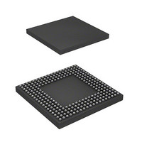
HD6417727BP100BV Renesas Electronics America, HD6417727BP100BV Datasheet - Page 860

HD6417727BP100BV
Manufacturer Part Number
HD6417727BP100BV
Description
IC SUPERH MPU ROMLESS 240BGA
Manufacturer
Renesas Electronics America
Series
SuperH® SH7700r
Datasheet
1.HD6417727BP100CV.pdf
(1098 pages)
Specifications of HD6417727BP100BV
Core Processor
SH-3 DSP
Core Size
32-Bit
Speed
100MHz
Connectivity
FIFO, SCI, SIO, SmartCard, USB
Peripherals
DMA, LCD, POR, WDT
Number Of I /o
104
Program Memory Type
ROMless
Ram Size
32K x 8
Voltage - Supply (vcc/vdd)
1.6 V ~ 2.05 V
Data Converters
A/D 6x10b; D/A 2x8b
Oscillator Type
Internal
Operating Temperature
-20°C ~ 75°C
Package / Case
240-BGA
Lead Free Status / RoHS Status
Contains lead / RoHS non-compliant
Eeprom Size
-
Program Memory Size
-
- Current page: 860 of 1098
- Download datasheet (7Mb)
Section 25 LCD Controller
25.3.5
The timing controller register is used to run the controller in a way that matches the display
resolution of the LCD module. The display resolution is set up in the LCDC horizontal number
character number register, LCDC horizontal synchronization signal register, LCDC vertical line
displayed number register, LCDC vertical total line number register, and LCDC vertical
synchronization signal register. The LCD current-alternating period for an STN or DSTN display
is set by using the LCDC ac modulation signal toggle line number register. The initial values in
these registers are typical settings for VGA (640 × 480 dots) on an STN or DSTN display.
The clock to be used is set with the LCD input clock register. The LCD module frame rate is
determined by the display interval + retrace line interval (non-display interval) for one screen set
in a size related register and the frequency of the clock used.
This LCDC has a V
of each vertical retrace line period (to be exact, at the beginning of the line after the last line of the
display). This function is set up by using the LCDC interrupt control register.
25.3.6
An LCD module normally requires a specific sequence for processing to do with the cutoff of the
input power supply. Settings in the LCDC power management mode register, LCDC power supply
sequence period register, and LCDC control register, in conjunction with the LCD power-supply
control pins (VCPWC, VEPWC, and DON), are used to provide processing of power-supply
control sequences that suits the requirements of the LCD module.
Figures 25.4 to 25.7 are summary timing charts for power-supply control sequences and table 25.5
is a summary of available power-supply control sequence periods.
Rev.6.00 Mar. 27, 2009 Page 802 of 1036
REJ09B0254-0600
Timing Controller Register
Power Management Registers
sync
interrupt function so that it is possible to issue an interrupt at the beginning
Related parts for HD6417727BP100BV
Image
Part Number
Description
Manufacturer
Datasheet
Request
R

Part Number:
Description:
KIT STARTER FOR M16C/29
Manufacturer:
Renesas Electronics America
Datasheet:

Part Number:
Description:
KIT STARTER FOR R8C/2D
Manufacturer:
Renesas Electronics America
Datasheet:

Part Number:
Description:
R0K33062P STARTER KIT
Manufacturer:
Renesas Electronics America
Datasheet:

Part Number:
Description:
KIT STARTER FOR R8C/23 E8A
Manufacturer:
Renesas Electronics America
Datasheet:

Part Number:
Description:
KIT STARTER FOR R8C/25
Manufacturer:
Renesas Electronics America
Datasheet:

Part Number:
Description:
KIT STARTER H8S2456 SHARPE DSPLY
Manufacturer:
Renesas Electronics America
Datasheet:

Part Number:
Description:
KIT STARTER FOR R8C38C
Manufacturer:
Renesas Electronics America
Datasheet:

Part Number:
Description:
KIT STARTER FOR R8C35C
Manufacturer:
Renesas Electronics America
Datasheet:

Part Number:
Description:
KIT STARTER FOR R8CL3AC+LCD APPS
Manufacturer:
Renesas Electronics America
Datasheet:

Part Number:
Description:
KIT STARTER FOR RX610
Manufacturer:
Renesas Electronics America
Datasheet:

Part Number:
Description:
KIT STARTER FOR R32C/118
Manufacturer:
Renesas Electronics America
Datasheet:

Part Number:
Description:
KIT DEV RSK-R8C/26-29
Manufacturer:
Renesas Electronics America
Datasheet:

Part Number:
Description:
KIT STARTER FOR SH7124
Manufacturer:
Renesas Electronics America
Datasheet:

Part Number:
Description:
KIT STARTER FOR H8SX/1622
Manufacturer:
Renesas Electronics America
Datasheet:

Part Number:
Description:
KIT DEV FOR SH7203
Manufacturer:
Renesas Electronics America
Datasheet:


