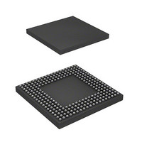
HD6417727BP100BV Renesas Electronics America, HD6417727BP100BV Datasheet - Page 555

HD6417727BP100BV
Manufacturer Part Number
HD6417727BP100BV
Description
IC SUPERH MPU ROMLESS 240BGA
Manufacturer
Renesas Electronics America
Series
SuperH® SH7700r
Datasheet
1.HD6417727BP100CV.pdf
(1098 pages)
Specifications of HD6417727BP100BV
Core Processor
SH-3 DSP
Core Size
32-Bit
Speed
100MHz
Connectivity
FIFO, SCI, SIO, SmartCard, USB
Peripherals
DMA, LCD, POR, WDT
Number Of I /o
104
Program Memory Type
ROMless
Ram Size
32K x 8
Voltage - Supply (vcc/vdd)
1.6 V ~ 2.05 V
Data Converters
A/D 6x10b; D/A 2x8b
Oscillator Type
Internal
Operating Temperature
-20°C ~ 75°C
Package / Case
240-BGA
Lead Free Status / RoHS Status
Contains lead / RoHS non-compliant
Eeprom Size
-
Program Memory Size
-
- Current page: 555 of 1098
- Download datasheet (7Mb)
Bit 4—Framing Error (FER): Indicates that data reception aborted due to a framing error in the
asynchronous mode.
Bit 4: FER
0
1
Notes: 1. Clearing the RE bit to 0 in the serial control register does not affect the FER bit, which
Bit 3—Parity Error (PER): Indicates that data reception (with parity) aborted due to a parity
error in the asynchronous mode.
Bit 3: PER
0
1
Notes: 1. Clearing the RE bit to 0 in the serial control register does not affect the PER bit, which
2. When the stop bit length is two bits, only the first bit is checked. The second stop bit is
2. When a parity error occurs, the SCI transfers the receive data into the SCRDR but does
retains its previous value.
not checked. When a framing error occurs, the SCI transfers the receive data into the
SCRDR but does not set RDRF. Serial receiving cannot continue while FER is set to 1.
In the clock synchronous mode, serial transmitting is also disabled.
retains its previous value.
not set RDRF. Serial receiving cannot continue while PER is set to 1. In the clock
synchronous mode, serial transmitting is also disabled.
Description
Receiving is in progress or has ended normally *
[Clear conditions]
1. When the chip is reset or enters standby mode
2. When FER=1 is read and then 0 is written to FER.
A receive framing error occurred
FER is set to 1 if the stop bit at the end of receive data is checked and found to
be 0. *
Description
Receiving is in progress or has ended normally *
[Clear conditions]
1. When the chip is reset or enters standby mode
2. When PER=1 is read and then 0 is written to PER.
A receive parity error occurred *
[Setting condition]
When the number of 1s in receive data, including the parity bit, does not match
the even or odd parity setting of the parity mode bit (O/E) in the serial mode
register (SCSMR).
2
Section 17 Serial Communication Interface (SCI)
2
Rev.6.00 Mar. 27, 2009 Page 497 of 1036
1
1
REJ09B0254-0600
(Initial value)
(Initial value)
Related parts for HD6417727BP100BV
Image
Part Number
Description
Manufacturer
Datasheet
Request
R

Part Number:
Description:
KIT STARTER FOR M16C/29
Manufacturer:
Renesas Electronics America
Datasheet:

Part Number:
Description:
KIT STARTER FOR R8C/2D
Manufacturer:
Renesas Electronics America
Datasheet:

Part Number:
Description:
R0K33062P STARTER KIT
Manufacturer:
Renesas Electronics America
Datasheet:

Part Number:
Description:
KIT STARTER FOR R8C/23 E8A
Manufacturer:
Renesas Electronics America
Datasheet:

Part Number:
Description:
KIT STARTER FOR R8C/25
Manufacturer:
Renesas Electronics America
Datasheet:

Part Number:
Description:
KIT STARTER H8S2456 SHARPE DSPLY
Manufacturer:
Renesas Electronics America
Datasheet:

Part Number:
Description:
KIT STARTER FOR R8C38C
Manufacturer:
Renesas Electronics America
Datasheet:

Part Number:
Description:
KIT STARTER FOR R8C35C
Manufacturer:
Renesas Electronics America
Datasheet:

Part Number:
Description:
KIT STARTER FOR R8CL3AC+LCD APPS
Manufacturer:
Renesas Electronics America
Datasheet:

Part Number:
Description:
KIT STARTER FOR RX610
Manufacturer:
Renesas Electronics America
Datasheet:

Part Number:
Description:
KIT STARTER FOR R32C/118
Manufacturer:
Renesas Electronics America
Datasheet:

Part Number:
Description:
KIT DEV RSK-R8C/26-29
Manufacturer:
Renesas Electronics America
Datasheet:

Part Number:
Description:
KIT STARTER FOR SH7124
Manufacturer:
Renesas Electronics America
Datasheet:

Part Number:
Description:
KIT STARTER FOR H8SX/1622
Manufacturer:
Renesas Electronics America
Datasheet:

Part Number:
Description:
KIT DEV FOR SH7203
Manufacturer:
Renesas Electronics America
Datasheet:


