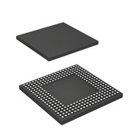
HD6417712BPV Renesas Electronics America, HD6417712BPV Datasheet - Page 609

HD6417712BPV
Manufacturer Part Number
HD6417712BPV
Description
MPU 1.5/3.3V 0K PB-FREE 256-BGA
Manufacturer
Renesas Electronics America
Series
SuperH® SH Ethernetr
Datasheet
1.HD6417712BPV.pdf
(980 pages)
Specifications of HD6417712BPV
Core Processor
SH-3 DSP
Core Size
32-Bit
Speed
200MHz
Connectivity
EBI/EMI, Ethernet, FIFO, SCI, SIO
Peripherals
DMA, POR, WDT
Number Of I /o
24
Program Memory Type
ROMless
Ram Size
16K x 8
Voltage - Supply (vcc/vdd)
1.4 V ~ 1.6 V
Oscillator Type
External
Operating Temperature
-20°C ~ 75°C
Package / Case
256-BGA
Lead Free Status / RoHS Status
Lead free / RoHS Compliant
Eeprom Size
-
Program Memory Size
-
Data Converters
-
Available stocks
Company
Part Number
Manufacturer
Quantity
Price
Company:
Part Number:
HD6417712BPV
Manufacturer:
Renesas Electronics America
Quantity:
10 000
- Current page: 609 of 980
- Download datasheet (6Mb)
Specify TxD pin as output port
set number) bytes of transmit
from TDFE bit and TEND flag
Clear TE bit in SCSCR to 0
Write (16 – transmit trigger
Read TEND bit in SCFSR
Read TDFE bit in SCFSR
in SCFSR, then clear to 0
data to SCFTDR, read 1
All data transmitted?
Start of transmission
End of transmission
Clear port DR to 0
Break output?
TEND = 1?
TDFE = 1?
by PFC
Figure 16.4 Sample Serial Transmission Flowchart
Yes
Yes
Yes
Yes
No
No
No
No
Section 16 Serial Communication Interface with FIFO (SCIF)
1. SCIF status check and transmit data write:
2. Serial transmission continuation procedure:
3. Break output at the end of serial
Read the serial status register (SCFSR)
and check that the TDFE flag is set to 1,
then write transmit data to SCFTDR, read 1
from the TDFE and TEND flags, then clear
these flags to 0.
The number of data bytes that can be
written is 16 – (transmit trigger set number).
To continue serial transmission, read 1
from the TDFE flag to confirm that writing is
possible, then write data to SCFTDR, and
then clear the TDFE bit to 0.
transmission:
To output a break in serial transmission,
clear the port data register (DR) to 0 before
clearing the TE bit in SCSCR to 0, and then
specify the TxD pin as an output port by the
PFC.
In steps 1 and 2, it is possible to ascertain
the number of data bytes that can be
written from the number of transmit data
bytes in SCFTDR indicated by the upper 8
bits of SCFDR.
Rev. 1.00 Dec. 27, 2005 Page 565 of 932
REJ09B0269-0100
Related parts for HD6417712BPV
Image
Part Number
Description
Manufacturer
Datasheet
Request
R

Part Number:
Description:
KIT STARTER FOR M16C/29
Manufacturer:
Renesas Electronics America
Datasheet:

Part Number:
Description:
KIT STARTER FOR R8C/2D
Manufacturer:
Renesas Electronics America
Datasheet:

Part Number:
Description:
R0K33062P STARTER KIT
Manufacturer:
Renesas Electronics America
Datasheet:

Part Number:
Description:
KIT STARTER FOR R8C/23 E8A
Manufacturer:
Renesas Electronics America
Datasheet:

Part Number:
Description:
KIT STARTER FOR R8C/25
Manufacturer:
Renesas Electronics America
Datasheet:

Part Number:
Description:
KIT STARTER H8S2456 SHARPE DSPLY
Manufacturer:
Renesas Electronics America
Datasheet:

Part Number:
Description:
KIT STARTER FOR R8C38C
Manufacturer:
Renesas Electronics America
Datasheet:

Part Number:
Description:
KIT STARTER FOR R8C35C
Manufacturer:
Renesas Electronics America
Datasheet:

Part Number:
Description:
KIT STARTER FOR R8CL3AC+LCD APPS
Manufacturer:
Renesas Electronics America
Datasheet:

Part Number:
Description:
KIT STARTER FOR RX610
Manufacturer:
Renesas Electronics America
Datasheet:

Part Number:
Description:
KIT STARTER FOR R32C/118
Manufacturer:
Renesas Electronics America
Datasheet:

Part Number:
Description:
KIT DEV RSK-R8C/26-29
Manufacturer:
Renesas Electronics America
Datasheet:

Part Number:
Description:
KIT STARTER FOR SH7124
Manufacturer:
Renesas Electronics America
Datasheet:

Part Number:
Description:
KIT STARTER FOR H8SX/1622
Manufacturer:
Renesas Electronics America
Datasheet:

Part Number:
Description:
KIT DEV FOR SH7203
Manufacturer:
Renesas Electronics America
Datasheet:


