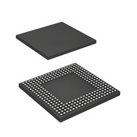
HD6417712BPV Renesas Electronics America, HD6417712BPV Datasheet - Page 73

HD6417712BPV
Manufacturer Part Number
HD6417712BPV
Description
MPU 1.5/3.3V 0K PB-FREE 256-BGA
Manufacturer
Renesas Electronics America
Series
SuperH® SH Ethernetr
Datasheet
1.HD6417712BPV.pdf
(980 pages)
Specifications of HD6417712BPV
Core Processor
SH-3 DSP
Core Size
32-Bit
Speed
200MHz
Connectivity
EBI/EMI, Ethernet, FIFO, SCI, SIO
Peripherals
DMA, POR, WDT
Number Of I /o
24
Program Memory Type
ROMless
Ram Size
16K x 8
Voltage - Supply (vcc/vdd)
1.4 V ~ 1.6 V
Oscillator Type
External
Operating Temperature
-20°C ~ 75°C
Package / Case
256-BGA
Lead Free Status / RoHS Status
Lead free / RoHS Compliant
Eeprom Size
-
Program Memory Size
-
Data Converters
-
Available stocks
Company
Part Number
Manufacturer
Quantity
Price
Company:
Part Number:
HD6417712BPV
Manufacturer:
Renesas Electronics America
Quantity:
10 000
- Current page: 73 of 980
- Download datasheet (6Mb)
2.2
2.2.1
The LSI supports 32-bit logical addresses and accesses system resources using the 4-Gbytes of
logical address space. User programs and data are accessed from the logical address space. The
logical address space is divided into several areas as shown in table 2.1.
P0/U0 Area: This area is called the P0 area when the CPU is in privileged mode and the U0 area
when in user mode. For the P0 and U0 areas, access using the cache is enabled. The P0 and U0
areas are handled as address translatable areas.
If the cache is enabled, access to the P0 or U0 area is cached. If a P0 or U0 address is specified
while the address translation unit is enabled, the P0 or U0 address is translated into a physical
address based on translation information defined by the user.
If the CPU is in user mode, only the U0 area can be accessed. If P1, P2, P3, or P4 is accessed in
user mode, a transition to an address error exception occurs.
P1 Area: The P1 area is defined as a cacheable but non-address translatable area. Normally,
programs executed at high speed in privileged mode, such as exception processing handlers, which
are at the core of the operating system (S), are assigned to the P1 area.
P2 Area: The P2 area is defined as a non-cacheable but non-address translatable area. A reset
processing program to be called from the reset state is described at the start address (H'A0000000)
of the P2 area. Normally, programs such as system initialization routines and OS initiation
programs are assigned to the P2 area. To access a part of an on-chip I/O, its corresponding
program should be assigned to the P2 area.
P3 Area: The P3 area is defined as a cacheable and address translatable area. This area is used if
an address translation is required for a privileged program.
P4 Area: The P4 area is defined as a control area which is non-cacheable and non-address
translatable. This area can be accessed only in privileged mode. A part of the LSI's on-chip I/O is
assigned to this area.
Memory Map
Logical Address Space
Rev. 1.00 Dec. 27, 2005 Page 29 of 932
REJ09B0269-0100
Section 2 CPU
Related parts for HD6417712BPV
Image
Part Number
Description
Manufacturer
Datasheet
Request
R

Part Number:
Description:
KIT STARTER FOR M16C/29
Manufacturer:
Renesas Electronics America
Datasheet:

Part Number:
Description:
KIT STARTER FOR R8C/2D
Manufacturer:
Renesas Electronics America
Datasheet:

Part Number:
Description:
R0K33062P STARTER KIT
Manufacturer:
Renesas Electronics America
Datasheet:

Part Number:
Description:
KIT STARTER FOR R8C/23 E8A
Manufacturer:
Renesas Electronics America
Datasheet:

Part Number:
Description:
KIT STARTER FOR R8C/25
Manufacturer:
Renesas Electronics America
Datasheet:

Part Number:
Description:
KIT STARTER H8S2456 SHARPE DSPLY
Manufacturer:
Renesas Electronics America
Datasheet:

Part Number:
Description:
KIT STARTER FOR R8C38C
Manufacturer:
Renesas Electronics America
Datasheet:

Part Number:
Description:
KIT STARTER FOR R8C35C
Manufacturer:
Renesas Electronics America
Datasheet:

Part Number:
Description:
KIT STARTER FOR R8CL3AC+LCD APPS
Manufacturer:
Renesas Electronics America
Datasheet:

Part Number:
Description:
KIT STARTER FOR RX610
Manufacturer:
Renesas Electronics America
Datasheet:

Part Number:
Description:
KIT STARTER FOR R32C/118
Manufacturer:
Renesas Electronics America
Datasheet:

Part Number:
Description:
KIT DEV RSK-R8C/26-29
Manufacturer:
Renesas Electronics America
Datasheet:

Part Number:
Description:
KIT STARTER FOR SH7124
Manufacturer:
Renesas Electronics America
Datasheet:

Part Number:
Description:
KIT STARTER FOR H8SX/1622
Manufacturer:
Renesas Electronics America
Datasheet:

Part Number:
Description:
KIT DEV FOR SH7203
Manufacturer:
Renesas Electronics America
Datasheet:


