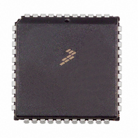
MC68HC705C9ACFN Freescale Semiconductor, MC68HC705C9ACFN Datasheet - Page 75

MC68HC705C9ACFN
Manufacturer Part Number
MC68HC705C9ACFN
Description
IC MCU 2.1MHZ 16K OTP 44-PLCC
Manufacturer
Freescale Semiconductor
Series
HC05r
Datasheet
1.MC705C9ACPE.pdf
(118 pages)
Specifications of MC68HC705C9ACFN
Core Processor
HC05
Core Size
8-Bit
Speed
2.1MHz
Connectivity
SCI, SPI
Peripherals
POR, WDT
Number Of I /o
24
Program Memory Size
16KB (16K x 8)
Program Memory Type
OTP
Ram Size
352 x 8
Voltage - Supply (vcc/vdd)
3 V ~ 5.5 V
Oscillator Type
Internal
Operating Temperature
-40°C ~ 85°C
Package / Case
44-PLCC
Lead Free Status / RoHS Status
Contains lead / RoHS non-compliant
Eeprom Size
-
Data Converters
-
Available stocks
Company
Part Number
Manufacturer
Quantity
Price
Company:
Part Number:
MC68HC705C9ACFN
Manufacturer:
Freescale Semiconductor
Quantity:
10 000
Company:
Part Number:
MC68HC705C9ACFNE
Manufacturer:
RFMD
Quantity:
8 729
Company:
Part Number:
MC68HC705C9ACFNE
Manufacturer:
Freescale Semiconductor
Quantity:
10 000
SPIE — Serial Peripheral Interrupt Enable Bit
SPE — Serial Peripheral System Enable Bit
DWOM — Port D Wire-OR Mode Option Bit
MSTR — Master Mode Select Bit
CPOL — Clock Polarity Bit
CPHA — Clock Phase Bit
SPR1 and SPR0 — SPI Clock Rate Selects
Freescale Semiconductor
This read/write bit enables SPI interrupts. Reset clears the SPIE bit.
This read/write bit enables the SPI. Reset clears the SPE bit.
This read/write bit disables the high side driver transistors on port D outputs so that port D outputs
become open-drain drivers. DWOM affects all seven port D pins together. This option is only available
when configured as a C9A.
This read/write bit selects master mode operation or slave mode operation. Reset clears the MSTR bit.
When the clock polarity bit is cleared and data is not being transferred, a steady state low value is
produced at the SCK pin of the master device. Conversely, if this bit is set, the SCK pin will idle high.
This bit is also used in conjunction with the clock phase control bit to produce the desired clock-data
relationship between master and slave. See
The clock phase bit, in conjunction with the CPOL bit, controls the clock-data relationship between
master and slave. The CPOL bit can be thought of as simply inserting an inverter in series with the
SCK line. The CPHA bit selects one of two fundamentally different clocking protocols. When
CPHA = 0, the shift clock is the OR of SCK with SS. As soon as SS goes low, the transaction begins
and the first edge on SCK invokes the first data sample. When CPHA=1, the SS pin may be thought
of as a simple output enable control. See
These read/write bits select one of four master mode serial clock rates, as shown in
have no effect in the slave mode.
1 = SPI interrupts enabled
0 = SPI interrupts disabled
1 = SPI system enabled
0 = SPI system disabled
1 = Port D outputs act as open-drain outputs.
0 = Port D outputs are normal CMOS outputs.
1 = Master mode
0 = Slave mode
$000A
Reset:
Read:
Write:
U = Undetermined
SPIE
Bit 7
0
MC68HC05C9A Advance Information Data Sheet, Rev. 4.1
Figure 10-4. SPI Control Register (SPCR)
SPE
6
0
DWOM
(C9A)
5
0
Figure
Figure
MSTR
4
0
10-1.
10-1.
CPOL
3
0
CPHA
2
1
SPR1
U
1
SPR0
Bit 0
Table
U
SPI Registers
10-1. They
75


