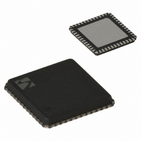
XE1203FI063TRLF Semtech, XE1203FI063TRLF Datasheet - Page 10

XE1203FI063TRLF
Manufacturer Part Number
XE1203FI063TRLF
Description
IC TXRX 433/868/915MHZ 48-VQFN
Manufacturer
Semtech
Specifications of XE1203FI063TRLF
Frequency
180MHz Center
Data Rate - Maximum
152.3kbps
Modulation Or Protocol
FSK
Applications
AMR, ISM, Home Automation, Process Control
Power - Output
0 ~ 15dBm
Sensitivity
-114dBm
Voltage - Supply
2.4 V ~ 3.6 V
Current - Receiving
14mA
Current - Transmitting
62mA
Data Interface
PCB, Surface Mount
Antenna Connector
PCB, Surface Mount
Operating Temperature
-40°C ~ 85°C
Package / Case
48-VQFN
Receiving Current
14mA
Transmitting Current
62mA
Data Rate
152.3Kbps
Modulation Type
FSK
No. Of Pins
48
Supply Voltage Range
2.4V To 3.6V
Operating Temperature Range
-40°C To +85°C
Operating Temperature (min)
-40C
Operating Temperature (max)
85C
Operating Temperature Classification
Industrial
Product Depth (mm)
7mm
Product Length (mm)
7mm
Operating Supply Voltage (typ)
2.5/3.3V
Operating Supply Voltage (max)
3.6V
Lead Free Status / RoHS Status
Lead free / RoHS Compliant
Memory Size
-
Lead Free Status / Rohs Status
Compliant
Other names
XE1203FI063TR
Available stocks
Company
Part Number
Manufacturer
Quantity
Price
Company:
Part Number:
XE1203FI063TRLF
Manufacturer:
SEMTECH
Quantity:
1 100
Company:
Part Number:
XE1203FI063TRLF
Manufacturer:
Semtech
Quantity:
2 300
Part Number:
XE1203FI063TRLF
Manufacturer:
SEMTECH/美国升特
Quantity:
20 000
4.1.5
4.1.6
4.1.7
The pin DATA is by default used by both the transmitter and the receiver sections. By default it is set as a
bidirectional I/O pin. When in receive mode, demodulated data appears at DATA as an output signal. In transmit
mode, the transmitted bit stream is applied to this pin as an input.
Some applications may require separate input and output pins for the transmitted and received data. In this case
the user has to set the ADParam_disable_data_bidir Configuration Register bit to ‘1’. As a result the DATA pin is
set as an output only for the received data, while the transmit data is controlled via the DATAIN input pin.
When in receiver mode, this feature is activated by setting RTParam_Pattern Configuration Register bit high. The
demodulated data signal is compared with a pattern stored in the PATParam_Pattern Configuration Register. The
PATTERN output pin is driven by the output of this comparator and is synchronized by DCLK. It is set to high when
a matching condition is detected, otherwise set to low. The PATTERN output is updated at the rising edge of
DCLK. The number of bits used for comparison is defined in the ADParam_Psize Configuration Register and the
number of tolerated errors for the pattern recognition is defined in the ADParam_Ptol register. Figure 4, below,
illustrates the pattern matching process.
When enabled, this function provides a Received Signal Strength Indication based on the signal at the output of the
base-band filter. To enable the RSSI function, the RTParam_RSSI Configuration Register bit should be set to “1”.
When enabled, the status of the RSSI in the DataOut_RSSI register is a 2-bit word which can be read via the serial
control interface. The content of the register is defined in Table 5, below, where V
equivalent to the RF input signal with the receiver operated in A-mode. The thresholds, V
the signal at the output of the base-band filter stage, divided by the signal gain.
Two possible ranges, each having a set of three V
actual values), are selected with the RTParam_RSSIR Configuration Register bit. They provide an overall RSSI
range of typically 25 dB.
The timing diagram of an RSSI measurement is illustrated in the Figure 5 below. When the RSSI function has been
activated, the signal strength is periodically measured and the result is stored in the register DataOut_RSSI each
time this DataOut_RSSI register is read via the 3-wire serial interface. Note that TS_RS is the wake-up time
required after the function has been enabled to ensure that a valid reading of RSSI is obtained.
© Semtech 2008
The DATA and DATAIN pins
Pattern recognition block
RSSI
DataOut_RSSI
0 0
0 1
1 0
1 1
Figure 4: Pattern Matching Operation.
Table 5 RSSI status description
TH
threshold values, VTHR1, VTHR2, and VTHR3 (see 3.2.2 for
VTHR1 < V
VTHR2 < V
10
V
VTHR3 < V
Description
RFFIL
≤ VTHR1
RFFIL
RFFIL
≤ VTHR2
≤ VTHR3
RFFIL
RFFIL
is the differential amplitude
TH
are the equivalent of
XE1203F
www.semtech.com


