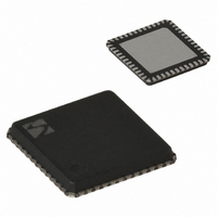
XE1203FI063TRLF Semtech, XE1203FI063TRLF Datasheet - Page 28

XE1203FI063TRLF
Manufacturer Part Number
XE1203FI063TRLF
Description
IC TXRX 433/868/915MHZ 48-VQFN
Manufacturer
Semtech
Specifications of XE1203FI063TRLF
Frequency
180MHz Center
Data Rate - Maximum
152.3kbps
Modulation Or Protocol
FSK
Applications
AMR, ISM, Home Automation, Process Control
Power - Output
0 ~ 15dBm
Sensitivity
-114dBm
Voltage - Supply
2.4 V ~ 3.6 V
Current - Receiving
14mA
Current - Transmitting
62mA
Data Interface
PCB, Surface Mount
Antenna Connector
PCB, Surface Mount
Operating Temperature
-40°C ~ 85°C
Package / Case
48-VQFN
Receiving Current
14mA
Transmitting Current
62mA
Data Rate
152.3Kbps
Modulation Type
FSK
No. Of Pins
48
Supply Voltage Range
2.4V To 3.6V
Operating Temperature Range
-40°C To +85°C
Operating Temperature (min)
-40C
Operating Temperature (max)
85C
Operating Temperature Classification
Industrial
Product Depth (mm)
7mm
Product Length (mm)
7mm
Operating Supply Voltage (typ)
2.5/3.3V
Operating Supply Voltage (max)
3.6V
Lead Free Status / RoHS Status
Lead free / RoHS Compliant
Memory Size
-
Lead Free Status / Rohs Status
Compliant
Other names
XE1203FI063TR
Available stocks
Company
Part Number
Manufacturer
Quantity
Price
Company:
Part Number:
XE1203FI063TRLF
Manufacturer:
SEMTECH
Quantity:
1 100
Company:
Part Number:
XE1203FI063TRLF
Manufacturer:
Semtech
Quantity:
2 300
Part Number:
XE1203FI063TRLF
Manufacturer:
SEMTECH/美国升特
Quantity:
20 000
5.2.8
5.3
5.3.1
Some settings in this 9-byte register can be used to have access to additional configurations of the circuit. These
settings are described in the Table 18 below:
The XE1203F has four main operating modes illustrated in Table 19 below.
These modes are defined by the content of the SWParam_mode_1 parameter when configuration set #1 is
selected, or by the content of the SWParam_mode_2 parameter when configuration set #2 is selected. See also
Section 5.2.1.
The XE1203F circuit can be switched between any configuration by using the 3 wire interface (ConfigSwitch) or by
using the pad SWITCH. This section describes the switching sequence of the chip. Figure 18 shows the transition
sequence from sleep mode to receiver mode via stand by mode.
© Semtech 2008
Mode
Sleep mode
Standby mode
Receiver mode
Transmitter mode
OPERATING MODES
TParam_HPF
TParam_BW
Test Registers and additional settings
Standard power up sequence for the receiver and transmitter
Name
SWParam_mode_2(1:0)
SWParam_mode1(1:0)
Bits
1-0
3
0 0
0 0
1 0
1 1
Table 18: Test registers and additional settings
Table 19: XE1203F Operating Modes
Byte Address
10111
10111
Description
-
Quartz oscillator enabled
Quartz oscillator, Frequency synthesizer, Receiver enabled
Quartz oscillator, Frequency synthesizer, Transmitter enabled
28
Description
Baseband filter bandwidth (DSB):
SSB cut-off frequency of the HPF stage
0 -> default values defined by
RTParam_BW (200 and 600 kHz)
1 -> 300kHz
(for cancellation of DC and low-frequency
offsets in the baseband circuit):
00 -> 4.3 kHz
01 -> 8.7 kHz
10 -> 17.3 kHz
11 -> 34.6 kHz
XE1203F
www.semtech.com


