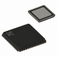
XE1203FI063TRLF Semtech, XE1203FI063TRLF Datasheet - Page 7

XE1203FI063TRLF
Manufacturer Part Number
XE1203FI063TRLF
Description
IC TXRX 433/868/915MHZ 48-VQFN
Manufacturer
Semtech
Specifications of XE1203FI063TRLF
Frequency
180MHz Center
Data Rate - Maximum
152.3kbps
Modulation Or Protocol
FSK
Applications
AMR, ISM, Home Automation, Process Control
Power - Output
0 ~ 15dBm
Sensitivity
-114dBm
Voltage - Supply
2.4 V ~ 3.6 V
Current - Receiving
14mA
Current - Transmitting
62mA
Data Interface
PCB, Surface Mount
Antenna Connector
PCB, Surface Mount
Operating Temperature
-40°C ~ 85°C
Package / Case
48-VQFN
Receiving Current
14mA
Transmitting Current
62mA
Data Rate
152.3Kbps
Modulation Type
FSK
No. Of Pins
48
Supply Voltage Range
2.4V To 3.6V
Operating Temperature Range
-40°C To +85°C
Operating Temperature (min)
-40C
Operating Temperature (max)
85C
Operating Temperature Classification
Industrial
Product Depth (mm)
7mm
Product Length (mm)
7mm
Operating Supply Voltage (typ)
2.5/3.3V
Operating Supply Voltage (max)
3.6V
Lead Free Status / RoHS Status
Lead free / RoHS Compliant
Memory Size
-
Lead Free Status / Rohs Status
Compliant
Other names
XE1203FI063TR
Available stocks
Company
Part Number
Manufacturer
Quantity
Price
Company:
Part Number:
XE1203FI063TRLF
Manufacturer:
SEMTECH
Quantity:
1 100
Company:
Part Number:
XE1203FI063TRLF
Manufacturer:
Semtech
Quantity:
2 300
Part Number:
XE1203FI063TRLF
Manufacturer:
SEMTECH/美国升特
Quantity:
20 000
4.1
4
The XE1203F is a direct conversion (Zero-IF) half-duplex data transceiver. The circuit operates in three different
ISM frequency bands (433 MHz, 868 MHz and 915 MHz) and uses 2-level FSK modulation/demodulation to
provide a complete transmission link. It is capable of operating at data rates between 1.2 and 152.3 kbit/s, making
it ideally suited for applications where high data rates are required. It also supports the Konnex standard where the
bit rate is 32.7 kbit/s. The device includes dedicated Barker encoder/decoder hardware that may be activated to
modulate/demodulate the transmitted signal to reduce in-band interferences.
The XE1203F is a highly programmable device – channel, bit rate, frequency deviation, output power, base band
filter bandwidth, sensitivity vs. linearity, RSSI feature, and many other parameters – which makes it extremely
flexible, to meet a large number of end user requirements.
The main functional blocks of the XE1203F are the receiver, the transmitter, the frequency synthesizer and some
service blocks. The device also includes a series of configuration and status registers. In a typical application, the
XE1203F is programmed by a microcontroller via the 3-wire serial bus SI, SO, SCK to write to and read from these
registers.
The Receiver converts the incoming 2-level FSK modulated signal into a synchronized bit stream.
The Transmitter performs the modulation of the carrier by an input bit stream and the transmission of the
modulated signal.
The Frequency Synthesizer generates the local oscillator (LO) signal for the receiver section as well as the
continuous phase FSK modulated signal for the transmitter section.
The Service Blocks provide the internal voltage and current sources and provide all the necessary functions for
the circuit to work properly.
The Configuration Registers are a set of variable-length registers that are used to store various settings to
operate the XE1203F transceiver circuit. They are listed below in Table 4. Refer to Section 5.2 for the detailed
descriptions of these registers. These registers are accessed in write or read mode through the 3-wire serial bus,
as described in Section 5.1.
Naming convention: throughout this document, each individual bit in a particular Configuration Register includes
the name of this register followed by a bit identifier. For example, RTParam_Band are the “Band” bits within the
RTParam register.
The Digital Interface provides internal control signals for the whole circuit according to the configuration register
settings.
The receiver converts the incoming 2-level FSK modulated signal into a synchronized bit stream. The receiver is
composed of a low-noise amplifier, two down-conversion mixers, two base band filters, two base band amplifiers,
two limiters, a demodulator and a bit synchronizer. The bit synchronizer translates the output of the demodulator
into a glitch-free bit stream available on the pin DATA. It also generates a synchronized clock, DCLK, which can be
© Semtech 2008
Name
ConfigSwitch
RTParam
FSParam
SWParam
DataOut
ADParam
Pattern
GENERAL DESCRIPTION
THE RECEIVER SECTION
Description
1-bit data to switch between 2 sets of user-predefined SWParam Configuration Registers
Receiver and transmitter parameters
LO, Bitrate, Deviation and other frequency parameters
Additional parameters
2 sets of user-predefined configuration registers
Status register which can be read through the 3-wire serial interface
Reference pattern for the “pattern recognition” feature
Table 4: Configuration Registers
7
XE1203F
www.semtech.com


