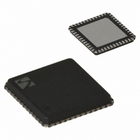
XE1203FI063TRLF Semtech, XE1203FI063TRLF Datasheet - Page 19

XE1203FI063TRLF
Manufacturer Part Number
XE1203FI063TRLF
Description
IC TXRX 433/868/915MHZ 48-VQFN
Manufacturer
Semtech
Specifications of XE1203FI063TRLF
Frequency
180MHz Center
Data Rate - Maximum
152.3kbps
Modulation Or Protocol
FSK
Applications
AMR, ISM, Home Automation, Process Control
Power - Output
0 ~ 15dBm
Sensitivity
-114dBm
Voltage - Supply
2.4 V ~ 3.6 V
Current - Receiving
14mA
Current - Transmitting
62mA
Data Interface
PCB, Surface Mount
Antenna Connector
PCB, Surface Mount
Operating Temperature
-40°C ~ 85°C
Package / Case
48-VQFN
Receiving Current
14mA
Transmitting Current
62mA
Data Rate
152.3Kbps
Modulation Type
FSK
No. Of Pins
48
Supply Voltage Range
2.4V To 3.6V
Operating Temperature Range
-40°C To +85°C
Operating Temperature (min)
-40C
Operating Temperature (max)
85C
Operating Temperature Classification
Industrial
Product Depth (mm)
7mm
Product Length (mm)
7mm
Operating Supply Voltage (typ)
2.5/3.3V
Operating Supply Voltage (max)
3.6V
Lead Free Status / RoHS Status
Lead free / RoHS Compliant
Memory Size
-
Lead Free Status / Rohs Status
Compliant
Other names
XE1203FI063TR
Available stocks
Company
Part Number
Manufacturer
Quantity
Price
Company:
Part Number:
XE1203FI063TRLF
Manufacturer:
SEMTECH
Quantity:
1 100
Company:
Part Number:
XE1203FI063TRLF
Manufacturer:
Semtech
Quantity:
2 300
Part Number:
XE1203FI063TRLF
Manufacturer:
SEMTECH/美国升特
Quantity:
20 000
The time diagram of a read sequence is illustrated in Figure 14
condition is detected, defined by the SI signal being set to “0” during a period of SCK. The next bit is a read/write
(R/W) bit which should be “1” to indicate a read operation. The next 5 bits are the address of the control register
A[4:0] to be accessed, MSB first. The data from the register is then output on the SO pin. The data become valid at
the rising edges of SCK and should be sampled at the falling edge of SCK. After this, the data transfer is
terminated. The SI line must stay high for at least one extra SCK clock cycle to start a new write or read sequence.
The maximum current drive on SO is 2 mA at a supply voltage of 2.7V and the maximum load is CLop, as defined
in Paragraph 3.2.2.
When the serial interface is not used for read or write operations, both SCK and SI should be set to “1”. Except
when in read mode, SO is set to a high impedance mode.
When reading the register at address zero, the timing diagram is illustrated in
© Semtech 2008
sck
si
/en
so
/en
so
si
sck
High impedance
Figure 13: Write sequence into configuration register at address zero
A(4) A(3) A(2) A(1)
Figure 14: Read sequence of configuration register
A(4)
A(0)
A(3)
D(7) D(6) D(5)
19
A(2)
High impedance
below. The sequence is initiated when a Start
A(1)
D(4) D(3)
A(0)
Figure 15.
D(2) D(1)
D(7)
D(0)
XE1203F
High impedance
www.semtech.com


