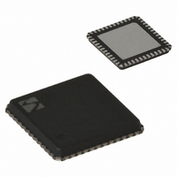
XE1203FI063TRLF Semtech, XE1203FI063TRLF Datasheet - Page 9

XE1203FI063TRLF
Manufacturer Part Number
XE1203FI063TRLF
Description
IC TXRX 433/868/915MHZ 48-VQFN
Manufacturer
Semtech
Specifications of XE1203FI063TRLF
Frequency
180MHz Center
Data Rate - Maximum
152.3kbps
Modulation Or Protocol
FSK
Applications
AMR, ISM, Home Automation, Process Control
Power - Output
0 ~ 15dBm
Sensitivity
-114dBm
Voltage - Supply
2.4 V ~ 3.6 V
Current - Receiving
14mA
Current - Transmitting
62mA
Data Interface
PCB, Surface Mount
Antenna Connector
PCB, Surface Mount
Operating Temperature
-40°C ~ 85°C
Package / Case
48-VQFN
Receiving Current
14mA
Transmitting Current
62mA
Data Rate
152.3Kbps
Modulation Type
FSK
No. Of Pins
48
Supply Voltage Range
2.4V To 3.6V
Operating Temperature Range
-40°C To +85°C
Operating Temperature (min)
-40C
Operating Temperature (max)
85C
Operating Temperature Classification
Industrial
Product Depth (mm)
7mm
Product Length (mm)
7mm
Operating Supply Voltage (typ)
2.5/3.3V
Operating Supply Voltage (max)
3.6V
Lead Free Status / RoHS Status
Lead free / RoHS Compliant
Memory Size
-
Lead Free Status / Rohs Status
Compliant
Other names
XE1203FI063TR
Available stocks
Company
Part Number
Manufacturer
Quantity
Price
Company:
Part Number:
XE1203FI063TRLF
Manufacturer:
SEMTECH
Quantity:
1 100
Company:
Part Number:
XE1203FI063TRLF
Manufacturer:
Semtech
Quantity:
2 300
Part Number:
XE1203FI063TRLF
Manufacturer:
SEMTECH/美国升特
Quantity:
20 000
4.1.4
demodulator output is directly connected to the DATA pin and the DCLK pin is set to low. Otherwise, the
demodulator output is processed by the bit synchronizer.
For correct operation of the demodulator the modulation index β of the input signal should meet the following
condition:
where Δf is the frequency deviation and BR the bit rate.
The raw output signal from the demodulator usually contains jitter and glitches. The bit synchronizer transforms the
data output of the demodulator into a glitch-free bit stream available on the DATA pin and generates a
synchronized clock DCLK to be used for sampling the DATA output (see Figure 3, below).
For proper operation, in addition to the requirement for the modulation index defined in 4.1.3 above, the Bit
Synchronizer must first receive three bytes of alternating logic value preamble, i.e. “0101” sequences. After this
startup phase, the rising edge of DCLK signal is centered on the demodulated bit. Subsequent data transitions will
preserve this centering.
This has two implications:
Number of Bits =
This implies approximately 6 consecutive unbalanced bytes when the Bit Rate precision is 1%, which is easily
achievable (crystal tolerance is in the range of 50 to 100 ppm). It is recommended that the bit rate accuracy be
better than ±5% (3% for Konnex mode operation).
The bit synchronizer is enabled when RTParam_Bsync Configuration Register bit is high. If this bit set low, the bit
synchronizer is disabled. In this case the output of the demodulator is directed to the DATA pin and the DCLK
output is set to “0”.
The received bit rate is defined by the value of the FSParam_BR Configuration Register, and is calculated as
follows:
Bit rate =
where int(x) is the integer value of the unsigned binary representation of (x).
Note: for Konnex standard operations, the bit rate is fixed at 32.7 kbit/s. ADParam_enable_konnex should be set to
a ‘1’.
© Semtech 2008
β
=
•
•
2
BR
Δ ⋅
Bit synchronizer
If the Bit Rates of Transmitter and Receiver are known to be the same, the XE1203F will be able to receive
an infinite unbalanced sequence (all “0s” or all ”1s”) with no restriction.
If there is a difference in Bit Rate between Tx and Rx, the amount of adjacent bits at the same level that
the BitSync can withstand can be estimated as:
f
int(FSPara
≥
, 2
DCLK
DATA
(NRZ)
152
m_BR(6
0.5
.
34
⋅
e
ΔBR
3
BR
:
0))
+
1
Figure 3: Bit synchronizer timing diagram.
9
XE1203F
www.semtech.com


