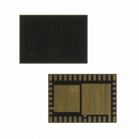
SI1015-A-GM Silicon Laboratories Inc, SI1015-A-GM Datasheet - Page 106

SI1015-A-GM
Manufacturer Part Number
SI1015-A-GM
Description
IC TXRX MCU + EZRADIOPRO
Manufacturer
Silicon Laboratories Inc
Specifications of SI1015-A-GM
Package / Case
42-QFN
Frequency
240MHz ~ 960MHz
Data Rate - Maximum
256kbps
Modulation Or Protocol
FSK, GFSK, OOK
Applications
General Purpose
Power - Output
13dBm
Sensitivity
-121dBm
Voltage - Supply
0.9 V ~ 3.6 V
Current - Receiving
18.5mA
Current - Transmitting
30mA
Data Interface
PCB, Surface Mount
Memory Size
8kB Flash, 768B RAM
Antenna Connector
PCB, Surface Mount
Number Of Receivers
1
Number Of Transmitters
1
Wireless Frequency
240 MHz to 960 MHz
Interface Type
UART, SMBus, SPI, PCA
Output Power
13 dBm
Operating Supply Voltage
0.9 V to 3.6 V
Maximum Operating Temperature
+ 85 C
Mounting Style
SMD/SMT
Maximum Supply Current
4 mA
Minimum Operating Temperature
- 40 C
Modulation
FSK, GFSK, OOK
Protocol Supported
C2, SMBus
Core
8051
Program Memory Type
Flash
Program Memory Size
8 KB
Data Ram Size
768 B
Supply Current (max)
4 mA
Lead Free Status / RoHS Status
Lead free / RoHS Compliant
Operating Temperature
-
Lead Free Status / Rohs Status
Lead free / RoHS Compliant
Other names
336-1868-5
Available stocks
Company
Part Number
Manufacturer
Quantity
Price
Company:
Part Number:
SI1015-A-GM
Manufacturer:
Silicon Labs
Quantity:
135
Part Number:
SI1015-A-GM
Manufacturer:
SILICONLA
Quantity:
20 000
- Current page: 106 of 384
- Download datasheet (3Mb)
Si1010/1/2/3/4/5
7.3. Comparator Response Time
Comparator response time may be configured in software via the CPTnMD registers described on
“CPT0MD: Comparator 0 Mode Selection” on page 108 and “CPT1MD: Comparator 1 Mode Selection” on
page 110. Four response time settings are available: Mode 0 (Fastest Response Time), Mode 1, Mode 2,
and Mode 3 (Lowest Power). Selecting a longer response time reduces the Comparator active supply cur-
rent. The Comparators also have low power shutdown state, which is entered any time the comparator is
disabled. Comparator rising edge and falling edge response times are typically not equal. See Table 4.14
on page 66 for complete comparator timing and supply current specifications.
7.4. Comparator Hysteresis
The Comparators feature software-programmable hysteresis that can be used to stabilize the comparator
output while a transition is occurring on the input. Using the CPTnCN registers, the user can program both
the amount of hysteresis voltage (referred to the input voltage) and the positive and negative-going sym-
metry of this hysteresis around the threshold voltage (i.e., the comparator negative input).
Figure 7.3 shows that when positive hysteresis is enabled, the comparator output does not transition from
logic 0 to logic 1 until the comparator positive input voltage has exceeded the threshold voltage by an
amount equal to the programmed hysteresis. It also shows that when negative hysteresis is enabled, the
comparator output does not transition from logic 1 to logic 0 until the comparator positive input voltage has
fallen below the threshold voltage by an amount equal to the programmed hysteresis.
The amount of positive hysteresis is determined by the settings of the CPnHYP bits in the CPTnCN regis-
ter and the amount of negative hysteresis voltage is determined by the settings of the CPnHYN bits in the
same register. Settings of 20, 10, 5, or 0 mV can be programmed for both positive and negative hysteresis.
See Section “Table 4.14. Comparator Electrical Characteristics” on page 66 for complete comparator hys-
teresis specifications.
106
(Programmed with CP0HYP Bits)
Positive Hysteresis Voltage
INPUTS
OUTPUT
VIN+
VIN-
CIRCUIT CONFIGURATION
Positive Hysteresis
CPn-
VIN+
CPn+
VIN-
Disabled
V
OL
V
OH
+
_
Figure 7.3. Comparator Hysteresis Plot
CPn
Positive Hysteresis
Maximum
OUT
Rev. 1.0
Negative Hysteresis
Disabled
Negative Hysteresis
(Programmed by CP0HYN Bits)
Maximum
Negative Hysteresis Voltage
Related parts for SI1015-A-GM
Image
Part Number
Description
Manufacturer
Datasheet
Request
R
Part Number:
Description:
SMD/C°/SINGLE-ENDED OUTPUT SILICON OSCILLATOR
Manufacturer:
Silicon Laboratories Inc
Part Number:
Description:
Manufacturer:
Silicon Laboratories Inc
Datasheet:
Part Number:
Description:
N/A N/A/SI4010 AES KEYFOB DEMO WITH LCD RX
Manufacturer:
Silicon Laboratories Inc
Datasheet:
Part Number:
Description:
N/A N/A/SI4010 SIMPLIFIED KEY FOB DEMO WITH LED RX
Manufacturer:
Silicon Laboratories Inc
Datasheet:
Part Number:
Description:
N/A/-40 TO 85 OC/EZLINK MODULE; F930/4432 HIGH BAND (REV E/B1)
Manufacturer:
Silicon Laboratories Inc
Part Number:
Description:
EZLink Module; F930/4432 Low Band (rev e/B1)
Manufacturer:
Silicon Laboratories Inc
Part Number:
Description:
I°/4460 10 DBM RADIO TEST CARD 434 MHZ
Manufacturer:
Silicon Laboratories Inc
Part Number:
Description:
I°/4461 14 DBM RADIO TEST CARD 868 MHZ
Manufacturer:
Silicon Laboratories Inc
Part Number:
Description:
I°/4463 20 DBM RFSWITCH RADIO TEST CARD 460 MHZ
Manufacturer:
Silicon Laboratories Inc
Part Number:
Description:
I°/4463 20 DBM RADIO TEST CARD 868 MHZ
Manufacturer:
Silicon Laboratories Inc
Part Number:
Description:
I°/4463 27 DBM RADIO TEST CARD 868 MHZ
Manufacturer:
Silicon Laboratories Inc
Part Number:
Description:
I°/4463 SKYWORKS 30 DBM RADIO TEST CARD 915 MHZ
Manufacturer:
Silicon Laboratories Inc
Part Number:
Description:
N/A N/A/-40 TO 85 OC/4463 RFMD 30 DBM RADIO TEST CARD 915 MHZ
Manufacturer:
Silicon Laboratories Inc
Part Number:
Description:
I°/4463 20 DBM RADIO TEST CARD 169 MHZ
Manufacturer:
Silicon Laboratories Inc


