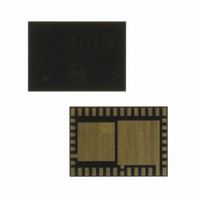
SI1015-A-GM Silicon Laboratories Inc, SI1015-A-GM Datasheet - Page 148

SI1015-A-GM
Manufacturer Part Number
SI1015-A-GM
Description
IC TXRX MCU + EZRADIOPRO
Manufacturer
Silicon Laboratories Inc
Specifications of SI1015-A-GM
Package / Case
42-QFN
Frequency
240MHz ~ 960MHz
Data Rate - Maximum
256kbps
Modulation Or Protocol
FSK, GFSK, OOK
Applications
General Purpose
Power - Output
13dBm
Sensitivity
-121dBm
Voltage - Supply
0.9 V ~ 3.6 V
Current - Receiving
18.5mA
Current - Transmitting
30mA
Data Interface
PCB, Surface Mount
Memory Size
8kB Flash, 768B RAM
Antenna Connector
PCB, Surface Mount
Number Of Receivers
1
Number Of Transmitters
1
Wireless Frequency
240 MHz to 960 MHz
Interface Type
UART, SMBus, SPI, PCA
Output Power
13 dBm
Operating Supply Voltage
0.9 V to 3.6 V
Maximum Operating Temperature
+ 85 C
Mounting Style
SMD/SMT
Maximum Supply Current
4 mA
Minimum Operating Temperature
- 40 C
Modulation
FSK, GFSK, OOK
Protocol Supported
C2, SMBus
Core
8051
Program Memory Type
Flash
Program Memory Size
8 KB
Data Ram Size
768 B
Supply Current (max)
4 mA
Lead Free Status / RoHS Status
Lead free / RoHS Compliant
Operating Temperature
-
Lead Free Status / Rohs Status
Lead free / RoHS Compliant
Other names
336-1868-5
Available stocks
Company
Part Number
Manufacturer
Quantity
Price
Company:
Part Number:
SI1015-A-GM
Manufacturer:
Silicon Labs
Quantity:
135
Part Number:
SI1015-A-GM
Manufacturer:
SILICONLA
Quantity:
20 000
- Current page: 148 of 384
- Download datasheet (3Mb)
Si1010/1/2/3/4/5
13.3. Security Options
The CIP-51 provides security options to protect the Flash memory from inadvertent modification by soft-
ware as well as to prevent the viewing of proprietary program code and constants. The Program Store
Write Enable (bit PSWE in register PSCTL) and the Program Store Erase Enable (bit PSEE in register
PSCTL) bits protect the Flash memory from accidental modification by software. PSWE must be explicitly
set to 1 before software can modify the Flash memory; both PSWE and PSEE must be set to 1 before soft-
ware can erase Flash memory. Additional security features prevent proprietary program code and data
constants from being read or altered across the C2 interface.
A Security Lock Byte located at the last byte of Flash user space offers protection of the Flash program
memory from access (reads, writes, or erases) by unprotected code or the C2 interface. The Flash security
mechanism allows the user to lock n 512-byte Flash pages, starting at page 0 (addresses 0x0000 to
0x01FF), where n is the 1s complement number represented by the Security Lock Byte. Note that the
page containing the Flash Security Lock Byte is unlocked when no other Flash pages are locked
(all bits of the Lock Byte are 1) and locked when any other Flash pages are locked (any bit of the
Lock Byte is 0).
The level of Flash security depends on the Flash access method. The three Flash access methods that
can be restricted are reads, writes, and erases from the C2 debug interface, user firmware executing on
unlocked pages, and user firmware executing on locked pages. Table 13.1 summarizes the Flash security
features of the Si1010/1/2/3/4/5 devices.
148
Security Lock Byte:
ones Complement:
Flash pages locked:
Addresses locked:
0x0000
0x3BFE
0xFFFF
0x3C00
0x3BFF
0x3A00
16KB Flash Device
Unlocked Flash Pages
Lock Byte Page
(SFLE = 0)
Lock Byte
Reserved
Figure 13.1. Flash Program Memory Map (16 kB and 8 kB devices)
0000 0100b
5 (First four Flash pages + Lock Byte Page)
0x0000 to 0x07FF (first four Flash pages) and
0x3A00 to 0x3BFF (Lock Byte Page)
Locked when
set according
security lock
Flash pages
1111 1011b
Access limit
to the Flash
are locked
any other
byte
Unlocked Flash Pages
8KB Flash Device
Lock Byte Page
Rev. 1.0
(SFLE = 0)
Lock Byte
Reserved
0xFFFF
0x2000
0x1FFF
0x1FFE
0x1E00
0x0000
16/8 KB Flash Device
Scratchpad Area
(Data Only)
(SFLE = 1)
0x01FF
0x0000
organized in
512-byte
memory
pages
Flash
Related parts for SI1015-A-GM
Image
Part Number
Description
Manufacturer
Datasheet
Request
R
Part Number:
Description:
SMD/C°/SINGLE-ENDED OUTPUT SILICON OSCILLATOR
Manufacturer:
Silicon Laboratories Inc
Part Number:
Description:
Manufacturer:
Silicon Laboratories Inc
Datasheet:
Part Number:
Description:
N/A N/A/SI4010 AES KEYFOB DEMO WITH LCD RX
Manufacturer:
Silicon Laboratories Inc
Datasheet:
Part Number:
Description:
N/A N/A/SI4010 SIMPLIFIED KEY FOB DEMO WITH LED RX
Manufacturer:
Silicon Laboratories Inc
Datasheet:
Part Number:
Description:
N/A/-40 TO 85 OC/EZLINK MODULE; F930/4432 HIGH BAND (REV E/B1)
Manufacturer:
Silicon Laboratories Inc
Part Number:
Description:
EZLink Module; F930/4432 Low Band (rev e/B1)
Manufacturer:
Silicon Laboratories Inc
Part Number:
Description:
I°/4460 10 DBM RADIO TEST CARD 434 MHZ
Manufacturer:
Silicon Laboratories Inc
Part Number:
Description:
I°/4461 14 DBM RADIO TEST CARD 868 MHZ
Manufacturer:
Silicon Laboratories Inc
Part Number:
Description:
I°/4463 20 DBM RFSWITCH RADIO TEST CARD 460 MHZ
Manufacturer:
Silicon Laboratories Inc
Part Number:
Description:
I°/4463 20 DBM RADIO TEST CARD 868 MHZ
Manufacturer:
Silicon Laboratories Inc
Part Number:
Description:
I°/4463 27 DBM RADIO TEST CARD 868 MHZ
Manufacturer:
Silicon Laboratories Inc
Part Number:
Description:
I°/4463 SKYWORKS 30 DBM RADIO TEST CARD 915 MHZ
Manufacturer:
Silicon Laboratories Inc
Part Number:
Description:
N/A N/A/-40 TO 85 OC/4463 RFMD 30 DBM RADIO TEST CARD 915 MHZ
Manufacturer:
Silicon Laboratories Inc
Part Number:
Description:
I°/4463 20 DBM RADIO TEST CARD 169 MHZ
Manufacturer:
Silicon Laboratories Inc


