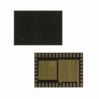
SI1015-A-GM Silicon Laboratories Inc, SI1015-A-GM Datasheet - Page 242

SI1015-A-GM
Manufacturer Part Number
SI1015-A-GM
Description
IC TXRX MCU + EZRADIOPRO
Manufacturer
Silicon Laboratories Inc
Specifications of SI1015-A-GM
Package / Case
42-QFN
Frequency
240MHz ~ 960MHz
Data Rate - Maximum
256kbps
Modulation Or Protocol
FSK, GFSK, OOK
Applications
General Purpose
Power - Output
13dBm
Sensitivity
-121dBm
Voltage - Supply
0.9 V ~ 3.6 V
Current - Receiving
18.5mA
Current - Transmitting
30mA
Data Interface
PCB, Surface Mount
Memory Size
8kB Flash, 768B RAM
Antenna Connector
PCB, Surface Mount
Number Of Receivers
1
Number Of Transmitters
1
Wireless Frequency
240 MHz to 960 MHz
Interface Type
UART, SMBus, SPI, PCA
Output Power
13 dBm
Operating Supply Voltage
0.9 V to 3.6 V
Maximum Operating Temperature
+ 85 C
Mounting Style
SMD/SMT
Maximum Supply Current
4 mA
Minimum Operating Temperature
- 40 C
Modulation
FSK, GFSK, OOK
Protocol Supported
C2, SMBus
Core
8051
Program Memory Type
Flash
Program Memory Size
8 KB
Data Ram Size
768 B
Supply Current (max)
4 mA
Lead Free Status / RoHS Status
Lead free / RoHS Compliant
Operating Temperature
-
Lead Free Status / Rohs Status
Lead free / RoHS Compliant
Other names
336-1868-5
Available stocks
Company
Part Number
Manufacturer
Quantity
Price
Company:
Part Number:
SI1015-A-GM
Manufacturer:
Silicon Labs
Quantity:
135
Part Number:
SI1015-A-GM
Manufacturer:
SILICONLA
Quantity:
20 000
- Current page: 242 of 384
- Download datasheet (3Mb)
SDO
SCLK
nSEL
SCLK
nSEL
SDI
SDI
MOSI
SCL
MISO
MOSI
SCL
NSS
NSS
Si1010/1/2/3/4/5
The SPI interface contains a burst read/write mode which allows for reading/writing sequential registers
without having to re-send the SPI address. When the NSS bit is held low while continuing to send SCK
pulses, the SPI interface will automatically increment the ADDR and read from/write to the next address.
An example burst write transaction is illustrated in Figure 22.4 and a burst read in Figure 22.5. As long as
NSS is held low, input data will be latched into the transceiver every eight SCK cycles.
242
First Bit
First Bit
RW
RW
=1
=0
A6
A6
A5
A5
A4
A4
A3
A3
Figure 22.4. SPI Timing—Burst Write Mode
Figure 22.5. SPI Timing—Burst Read Mode
A2
A2
A1
A1
First Bit
A0
A0
D7
=X
D7
D7
=X
D6 D5 D4 D3
D6
=X
D6
=X
D5
=X
D5
=X
Rev. 1.0
D4
=X
D4
=X
D3
=X
D3
=X
D2
=X
D2
=X
D2 D1 D0
Last Bit
D1
=X
D1
=X
D0
=X
D0
=X
D7
=X
D7 D6 D5 D4 D3
D6
=X
D5
=X
D4
=X
D3
=X
D2
=X
D2 D1 D0
D1
=X
Last Bit
D0
=X
Related parts for SI1015-A-GM
Image
Part Number
Description
Manufacturer
Datasheet
Request
R
Part Number:
Description:
SMD/C°/SINGLE-ENDED OUTPUT SILICON OSCILLATOR
Manufacturer:
Silicon Laboratories Inc
Part Number:
Description:
Manufacturer:
Silicon Laboratories Inc
Datasheet:
Part Number:
Description:
N/A N/A/SI4010 AES KEYFOB DEMO WITH LCD RX
Manufacturer:
Silicon Laboratories Inc
Datasheet:
Part Number:
Description:
N/A N/A/SI4010 SIMPLIFIED KEY FOB DEMO WITH LED RX
Manufacturer:
Silicon Laboratories Inc
Datasheet:
Part Number:
Description:
N/A/-40 TO 85 OC/EZLINK MODULE; F930/4432 HIGH BAND (REV E/B1)
Manufacturer:
Silicon Laboratories Inc
Part Number:
Description:
EZLink Module; F930/4432 Low Band (rev e/B1)
Manufacturer:
Silicon Laboratories Inc
Part Number:
Description:
I°/4460 10 DBM RADIO TEST CARD 434 MHZ
Manufacturer:
Silicon Laboratories Inc
Part Number:
Description:
I°/4461 14 DBM RADIO TEST CARD 868 MHZ
Manufacturer:
Silicon Laboratories Inc
Part Number:
Description:
I°/4463 20 DBM RFSWITCH RADIO TEST CARD 460 MHZ
Manufacturer:
Silicon Laboratories Inc
Part Number:
Description:
I°/4463 20 DBM RADIO TEST CARD 868 MHZ
Manufacturer:
Silicon Laboratories Inc
Part Number:
Description:
I°/4463 27 DBM RADIO TEST CARD 868 MHZ
Manufacturer:
Silicon Laboratories Inc
Part Number:
Description:
I°/4463 SKYWORKS 30 DBM RADIO TEST CARD 915 MHZ
Manufacturer:
Silicon Laboratories Inc
Part Number:
Description:
N/A N/A/-40 TO 85 OC/4463 RFMD 30 DBM RADIO TEST CARD 915 MHZ
Manufacturer:
Silicon Laboratories Inc
Part Number:
Description:
I°/4463 20 DBM RADIO TEST CARD 169 MHZ
Manufacturer:
Silicon Laboratories Inc


