DEIC420 IXYS RF, DEIC420 Datasheet

IC, RF MOSFET DRIVER, LOW SIDE, DE275-6

DEIC420

Manufacturer Part Number
DEIC420
Description
IC, RF MOSFET DRIVER, LOW SIDE, DE275-6
Manufacturer
IXYS RF
Datasheet

Specifications of DEIC420

Device Type
Low Side
Module Configuration
Low Side
Peak Output Current
20A
Output Resistance
0.4ohm
Input Delay
32ns
Output Delay
29ns
Supply Voltage Range
8V To 30V
Lead Free Status / RoHS Status
Lead free / RoHS Compliant
Features
• Built using the advantages and compatibility
• Latch-Up Protected
• High Peak Output Current: 20A Peak
• Wide Operating Range: 8V to 30V
• Rise And Fall Times of <4ns
• Minimum Pulse Width Of 8ns
• High Capacitive Load
• Matched Rise And Fall Times
• 32ns Input To Output Delay Time
• Low Output Impedance
• Low Quiescent Supply Currentt
Applications
• Driving RF MOSFETs
• Class D or E Switching Amplifier Drivers
• Multi MHz Switch Mode Power Supplies (SMPS)
• Pulse Generators
• Acoustic Transducer Drivers
• Pulsed Laser Diode Drivers
• DC to DC Converters
• Pulse Transformer Driver
Copyright © DIRECTED ENERGY, INC. 2001, 2002
Figure 1 - DEIC420 Functional Diagram
of CMOS and IXYS HDMOS
Drive Capability: 4nF in <4ns
TM
DEIC420
20 Ampere Low-Side Ultrafast RF MOSFET Driver
processes
Description
TheDEIC420 is a CMOS high speed high current gate
driver specifically designed to drive MOSFETs in Class D
and E HF RF applications at up to 45MHz, as well as
other applications requiring ultrafast rise and fall times or
short minimum pulse widths. The DEIC420 can source
and sink 20A of peak current while producing voltage rise
and fall times of less than 4ns, and minimum pulse
widths of 8ns. The input of the driver is compatible with
TTL or CMOS and is fully immune to latch up over the
entire operating range. Designed with small internal
delays, cross conduction/current shoot-through is
virtually eliminated in the DEIC420. Its features and wide
safety margin in operating voltage and power make the
DEIC420 unmatched in performance and value.
The DEIC420 is packaged in DEI's low inductance RF
package incorporating DEI's patented
techniques to minimize stray lead inductances for
optimum switching performance. For applications that do
not require the power dissipation of the DEIC420, the
driver is also available in a 28 pin SOIC package. See
the IXDD415SI data sheet for additional information. The
DEIC420 is a surface-mount device, and incorporates
patented RF layout techniques to minimize stray lead
inductances for optimum switching performance.
(1)
DEI U.S. Patent #4,891,686
First Release
(1)
RF layout

Related parts for DEIC420

DEIC420 Summary of contents

Page 1

... DEI's patented techniques to minimize stray lead inductances for optimum switching performance. For applications that do not require the power dissipation of the DEIC420, the driver is also available pin SOIC package. See the IXDD415SI data sheet for additional information. The DEIC420 is a surface-mount device, and incorporates patented RF layout techniques to minimize stray lead inductances for optimum switching performance ...

Page 2

... CASE - 150 o C Storage Temperature Soldering Lead Temperature 300 o C (10 seconds maximum) Electrical Characteristics Unless otherwise noted All voltage measurements with respect to DGND. DEIC420 configured as described in Test Conditions. Symbol Parameter V High input voltage IH V Low input voltage IL V Input voltage range IN ...
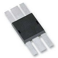
Page 3

... The guaranteed specifications apply only for the test conditions listed. Exposure to absolute maximum rated conditions for extended periods may affect device reliability. CAUTION: These devices are sensitive to electrostatic discharge; follow proper ESD procedures when handling and assembling this component. Figure 2 - DEIC420 Package Photo And Outline Figure 3a - Characteristics Test Diagram V IN DESCRIPTION Positive power-supply voltage input ...

Page 4

... Fig =4nF V =15V ONDLY OFFDLY Input Voltage (V) Fig Fig Fig DEIC420 Fall Time vs. Load Capacitance V = 15V 12V Load Capacitance (pF) Supply Current vs. Load Capacitance Vcc=15V 10 40 MHz 30 MHz 20 MHz 1 10 MHz 5 MHz 1 MHz 0 Load Capacitance (pF) Propagation Delay Times vs. Junction Temperature C = 4nF 15V ...

Page 5

... Unless otherwise noted, all waveforms are taken driving a 1nF load, 1MHz repetition frequency, V Figure 11 3ns Rise Time Figure 13 <8ns Minimum Pulse Width t ONDLY t OFFDLY 16 18 Typical Output Waveforms Figure 12 Figure 14 5 DEIC420 =15V, Case Temperature = 3ns Fall Time 1MHz CW Repetition Frequency ...

Page 6

... Figure 15 13.56MHz CW Repetition Frequency Figure 17 - High Frequency Gate Drive Circuit Figure 16 50MHz Burst Repetition Frequency 6 DEIC420 ...

Page 7

... Vcc Bypassing In order for the circuit to turn the MOSFET on properly, the DEIC420 must be able to draw up to 20A of current from the Vcc power supply in 2-6ns (depending upon the input capacitance of the MOSFET being driven). This means that there must be very low impedance between the driver and the power supply ...

Related keywords