DEIC515 IXYS RF, DEIC515 Datasheet

IC, RF MOSFET DRIVER LOW SIDE DE150IC-10

DEIC515

Manufacturer Part Number
DEIC515
Description
IC, RF MOSFET DRIVER LOW SIDE DE150IC-10
Manufacturer
IXYS RF
Datasheet

Specifications of DEIC515

Device Type
Low Side
Module Configuration
Low Side
Peak Output Current
15A
Output Resistance
0.5ohm
Input Delay
17.4ns
Output Delay
14.6ns
Supply Voltage Range
8V To 30V
Lead Free Status / RoHS Status
Lead free / RoHS Compliant

Available stocks

Company
Part Number
Manufacturer
Quantity
Price
Part Number:
DEIC515
Manufacturer:
ATMEL
Quantity:
1 100
Features
• Built using the advantages and compatibility
• Latch-Up Protected
• High Peak Output Current: 15A Peak
• Wide Operating Range: 8V to 30V
• Rise And Fall Times of <4ns
• Minimum Pulse Width Of 8ns
• High Capacitive Load
• Matched Rise And Fall Times
• 18ns Input To Output Delay Time
• Low Output Impedance
• Low Quiescent Supply Currentt
Applications
• Driving RF MOSFETs
• Class D or E Switching Amplifier Drivers
• Multi MHz Switch Mode Power Supplies (SMPS)
• Pulse Generators
• Acoustic Transducer Drivers
• Pulsed Laser Diode Drivers
• DC to DC Converters
• Pulse Transformer Driver
Figure 1 - DEIC515 Functional Diagram
of CMOS and IXYS HDMOS
Drive Capability: 2nF in <4ns
IN GND
VCC IN
IN
TM
processes
15 Ampere Low-Side Ultrafast RF MOSFET Driver
Description
TheDEIC515 is a CMOS high speed high current gate
driver specifically designed to drive MOSFETs in Class
D and E HF RF applications at up to 45MHz, as well as
other applications requiring ultrafast rise and fall times or
short minimum pulse widths. The DEIC515 can source
and sink 15A of peak current while producing voltage
rise and fall times of less than 4ns, and minimum pulse
widths of 8ns. The input of the driver is fully immune to
latch up over the entire operating range. Designed with
small internal delays, cross conduction/current shoot-
through is virtually eliminated in the DEIC515. Its
features and wide safety margin in operating voltage
and power make the DEIC515 unmatched in
performance and value.
The DEIC515 is packaged in DEI's low inductance RF
package incorporating DEI's patented
techniques to minimize stray lead inductances for
optimum switching performance. The DEIC515 is a
surface-mount device.
(1)
DEI U.S. Patent #4,891,686
DEIC515
(1)
RF layout
DGND
VCC
OUT

Related parts for DEIC515

DEIC515 Summary of contents

Page 1

... IN IN GND 15 Ampere Low-Side Ultrafast RF MOSFET Driver Description TheDEIC515 is a CMOS high speed high current gate driver specifically designed to drive MOSFETs in Class D and applications 45MHz, as well as other applications requiring ultrafast rise and fall times or short minimum pulse widths. The DEIC515 can source ...

Page 2

... Storage Temperature -40C to 150C Soldering Lead Temperature 300C (10 seconds maximum) Electrical Characteristics Unless otherwise noted < All voltage measurements with respect to DGND. DEIC515 configured as described in Test Conditions. Symbol Parameter High input voltage Low input voltage IL V Input voltage range IN I Input current ...

Page 3

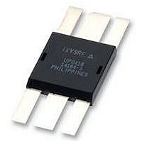
... The guaranteed specifications apply only for the test conditions listed. Exposure CAUTION: These devices are sensitive to electrostatic discharge; follow proper ESD procedures when handling and assembling this component. Figure 2 - DEIC515 Package Photo And Outline 15 Ampere Low-Side Ultrafast RF MOSFET Driver DESCRIPTION Input for the positive output section power-supply voltage ...

Page 4

... The very high currents and high speeds inside the DEIC515 create very large transients. To avoid problems with false triggering, the input to the DEIC515 should be supplied via a common mode choke. This is a simple tri-filar winding on a small ferrite core. This prevents high speed transients from effecting the input signals, by allowing the input signals to follow the internal die potential changes without changing the state of the input ...

Related keywords